As a promising high χ BCP for sub-20 nm patterning, PS-b-P2VP can easily form through-film lamellae nanostructure on silicon substrate by solvent annealing. PS-b-P2VP different molecular weights has different pitch sizes. By blending PS-b-P2VP polymers of different molecular weights, it is possible to tune the pitch size of a specific PS-b-P2VP continuously within a certain range.
The lamellar PS-b-P2VP thin film can be converted into a metal oxide hard mask through SIS process, in which the metal oxide (e.g AlOx) will selectively deposit in P2VP domain. This metal oxide mask can be used to visualize the lamellae pattern under SEM.
In our experiments, triblock copolymer VSV 12k-24k-12k (PDI=1.25), VSV 6.7k-13k-6.7k (PDI=1.26) and diblock copolymer SV 8.2k-8.3k (PDI=1.09) were used for blending. A poly(styrene-rand-2-vinylpridine-rand-hydroxyethyl methacrylate) (P(S-r-2VP-r-HEMA)) random copolymer with 60% styrene contain was used as the neutral brush. The VSV (12k-24k-12k) was blended with VSV (6.7k-13k-6.7k) or SV (8.2k-8.3k) at different volume ratios (10:0.5, 10:1, 10:1.5, 10:2). The self-assembly process of the as-blended VSV/SV and VSV/VSV films was as follows. First, the neutral brush was directly spin-coated on the silicon substrate, annealed at 200 °C for 1 hr. The role of the neutral brush is to help VSV form lamellar structure perpendicular to the substrate. The blended VSV/SV or VSV/VSV film was then coated on the neutral brush and solvent annealed in acetone. Acetone was chosen as the annealing agent because it was a neutral solvent to both PS and P2VP blocks. The blended films were kept in the annealing chamber with controlled amount of acetone vapor (with nitrogen as carrier gas, 5-100 sccm) at room temperature (25°C). To characterize the as-annealed films, sequential infiltration synthesis (SIS) process was employed to selectively deposit AlOx into P2VP domain. After SIS, the polymer was removed by reactive ion etching (RIE) and the remaining AlOx lines represented the self-assembled fingerprint pattern of the blended films. The images of the VSV films after different processes (SIS and etching) were taken by scanning electron microscopy (SEM).
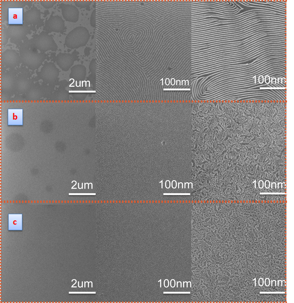
Figure 1 shows the SEM images of solvent annealing VSV (12k-24k-12k), VSV (6.7k-13k-6.7k) and SV (8.2k-8.3k) films after SIS process and RIE etching. It is found that VSV (12k-24k-12k) form very clear fingerprint pattern after solvent annealing, with a pitch size of 20.9 nm. However, for VSV (6.7k-13k-6.7k) and SV (8.2k-8.3k), no clear fingerprint patterns were formed after same processing conditions.
Figure 1.
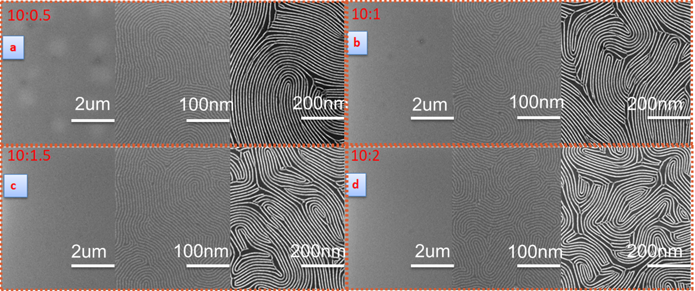
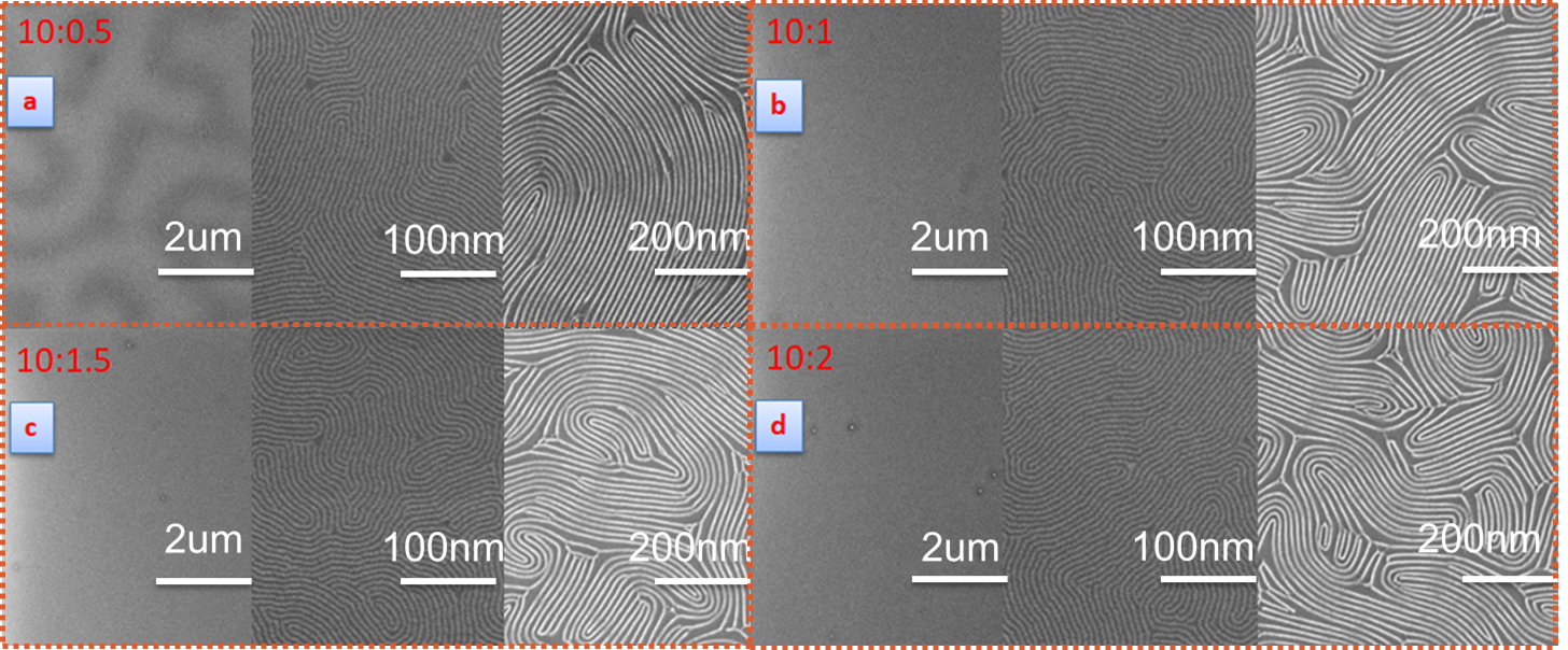
Microscopic characterization of polymer thin films of VSV (12k-24k-12k), VSV (6.7k-13k-6.7k) and SV (8.2k-8.3k) without blending. (a) VSV (12k-24k-12k); (b) VSV (6.7k-13k-6.7k); (c) SV (8.2k-8.3k). Each row (from left to right): a macroscopic to view of the whole film, an SEM image of the thin film after solvent annealing and SIS process, an SEM image after polymer removal with O2 plasma etching. In the BCP blending experiment, the triblock copolymer VSV (12k-24k-12k) was blended with diblock copolymer SV (8.2k-8.3k) or VSV (6.7k-13k-6.7k) at different volume ratios (10:0.5, 10:1, 10:1.5, 10:2) and annealed in acetone. From the SEM images shown in Figure 2, the VSV/SV films of all blending ratios self-assemble into lamellar fingerprint patterns, with a pitch size varying from 19.7 nm to 20.8 nm. After RIE etching, the AlOx lines clearly reproduce the fingerprint patterns, with correlation length varying from 138 nm to 40.5 nm. In the case of VSV/VSV blending, again it was observed that VSV/VSV films successfully form lamellar fingerprint patterns at different blending ratios. The pitch size of blended VSV/VSV changed from 20 nm at 10:2 to 20.7 nm at 10:0.5 (Figure 3). The correlation length of the blended VSV/VSV films lied in the range of 68 nm to 173 nm.
The pitch tuning capability of blending different BCPs is based on the molecular interactions between different BCP blocks. The blending process reconstruct the constituent blocks of the as-blended BCP, and therefore change the effective domain size of the as-blended BCP. By adding different polymers, the pitch size can be tuned in different range, as demonstrated in Figure 2 and Figure 3. Compare the two blending experiments, it is observed that blending VSV with SV results in larger pitch tuning range compared with VSV/VSV blending due to the stronger interaction between VSV and SV molecules.
Figure 2.
SEM images of VSV (12k-24k-12k)/SV (8.2k-8.3k) films of different blending ratios after solvent annealing and SIS process. (a) VSV/SV 10:0.5; (b) VSV/SV 10:1; (c) VSV/SV 10:1.5; (d) VSV/SV 10:2. Each row (from left to right): a macroscopic to view of the whole film (left), an SEM image of the thin film after solvent annealing and SIS process (middle), an SEM image after polymer removal with O2 plasma etching (right). Figure 3.
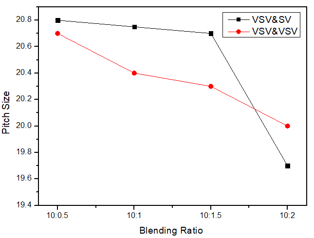
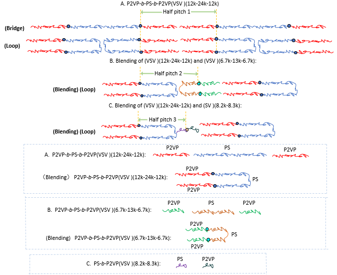
SEM images of VSV (12k-24k-12k)/ VSV (6.7k-13k-6.7k) films of different blending ratios after solvent annealing and SIS process. (a) VSV/VSV 10:0.5; (b) VSV/VSV 10:1, (c) VSV/VSV 10:1.5 (d) VSV/VSV 10:2. Each row (from left to right): a macroscopic to view of the whole film (left), an SEM image of the thin film after solvent annealing and SIS process (middle), an SEM image after polymer removal with O2 plasma etching (right). From the BCP blending experiments, the triblock copolymer VSV (12k-24k-12k) was blended with diblock copolymer SV (8.2k-8.3k) or VSV (6.7k-13k-6.7k) at different volume ratios (10:0.5, 10:1, 10:1.5, 10:2) and annealed in acetone. The pitch size versus the different volume ratios of VSV/ SV or VSV/VSV blending is shown in Figure 4. As the volume fraction of SV (8.2k-8.3k)or VSV (6.7k-13k-6.7k) increases, the pitch size of VSV (12k-24k-12k) after blending aslo decreases. Simultaneously, we can further explain from the chain mechanism of block copolymers why the pitch size decreases after blengding (VSV/ SV or VSV/VSV). The schematic diagram of VSV/ SV or VSV/VSV blending is shown in Figure 5 which is including “Half pitch 3 < Half pitch 2< Half pitch 1” in different volume fraction.
Figure 4.
The relationship between the vitrified pitch size and the different blending ratios (in volume) of VSV/ SV or VSV/VSV blending. Figure 5.
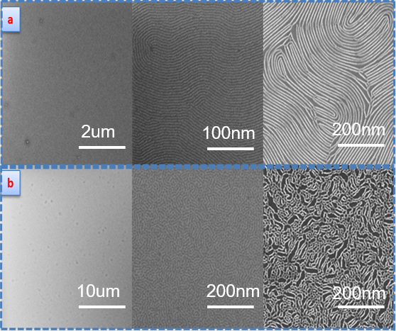
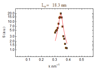
The schematic diagram illustrates the arrangement of polymer chains of the blended VSV/ SV or VSV/VSV. To explore the extreme blending conditions, as is shown in Figure 6. VSV (12k-24k-12k) was mixed with VSV (6.7k-13k-6.7k) and SV (8.2k-8.3k) respectively at 1:1 volume ratio. After same solvent annealing process, it was observed that VSV/SV (1:1) can still form good quality fingerprint pattern with pitch size of 18.3 nm (correlation length 164 nm). The pitch size plotting of quantitative effect of blending is shown in Figure 7. However, in case of VSV/SV at 1:1 blending ratio, the film was nearly in disordered status after annealing. Even though VSV/SV blending can achieve larger pitch tuning range, VSV/VSV blending has much larger processing window, with effective blending ratio range from 10:0.5 to 1:1.
Figure 6.
SEM images of VSV (12k-24k-12k)/ VSV (6.7k-13k-6.7k) films and VSV (12k-24k-12k)/ SV (8.2k-8.3k) films at 1:1 volume ratio. (a) VSV/VSV blending at 1:1 volume ratio. (b) VSV/SV blending at 1:1 volume ratio. Each row (from left to right): a macroscopic to view of the whole film, an SEM image of the thin film after solvent annealing and SIS process, an SEM image after polymer removal with O2 plasma etching. Figure 7.
The power density spectrum shows the pitch size of VSV/SV at 1:1 blending ratio. 

