Research Article Archive Versions 2 Vol 2 (4) : 19020407 2019
Download
White Light Interference Solution for Novel 3D NAND VIA Dishing Metrology
: 2019 - 10 - 17
: 2019 - 12 - 25
1776 25 0
Abstract & Keywords
Abstract: In traditional 3D NAND design, peripheral circuit accounts for 20-30% of the chip real-estate, which reduces the memory density of flash memory. As 3D NAND technology stacks to 128 layers or higher, peripheral circuits may account for more than 50% of the overall chip area. On the contrast, the XtackingTM technology arranges array and logic parts on two different wafers, and connects the memory arrays to the logic circuit by metal VIAs (Vertical Interconnect Accesses) to achieve unprecedented high storage density as well as DRAM level I/O speed. As a consequence, it becomes increasingly significant to monitor metal VIAs depth before wafer bonding process as to ensure reliability of array-logic connections. Currently, AFM (Atom Force Microscopy) is the main stream method of VIA depth monitoring. Apparently, AFM wins the battle of precision, however the low throughput limited its usage in mass production. In order to accomplish the requirement of VLSI production, a WLI (White Light Interference) metrology is revisited and a novel WLI method was developed to monitor VIAs depth. Basically there are two major limitations that keep WLI tools from wider use, transparent film impact and diffraction limitation. In this work, the engineering solutions are illustrated and inline dishing measurement is achieved with high accuracy and precision.
Keywords: WLI; Dishing; Metrology; 3D NAND; Bonding
1.   Introduction
In the XtackingTM technology, memory arrays and logic circuits are fabricated on separated wafers respectively and electrically connected by metal VIAs through a wafer bonding process [1]. Prior to wafer bonding, the bonding interfaces are created through a CMP (Chemical Mechanical Planarization) process. Over-polish strategy is universally applied to guarantee that metal diffusion is strictly controlled, thus to ensure high reliability. In this manner, the surface of metal VIA results in a dishing shape and its depth becomes a critical index of wafer-to-wafer connection. Therefore, a suitable monitoring scheme for VIA dishing is necessary to avoid structural and reliability issues such as interconnection open, metal void, metal diffusion, etc. Due to the requirement of good interconnection, the window for depth of VIA dishing is extremely narrow, and the requirement of metrology precision is critical. AFM, which has high precision is currently the major method to monitor dishing depth. Our previous work studied the utilization of AFM metrology and solution for ultra-precise measurement using pattern-centric method [2]. Yet the long measurement duration severely limits the application of AFM in mass production. Among height related measurement methods, white light interferometer offers an alternative option. In brief, white light interferometer provides high precision by using optical phase-shifting techniques, and a broad spectral width light source is generally applied in order to increase dynamic range of measurement [3]. The advantage is obvious since, although a vertical scanning is mandatory to collect interference fringes, the field data with less than 100 nm per pixel resolution is obtained spontaneously, which greatly reduces measurement duration. As a result, WLI is more than 100 times faster than line-scanning AFM in the same measurement.
On the other hand, there are also two bottlenecks that keep WLI from wider use in real time wafer metrology. Firstly, multiple-layer reflection caused by transparent films stack has a large impact on the interference fringes since it shifts the wave phase and derives inauthentic height. Secondly, the resolution is determined by the diffraction limit. Due to the limitation of interference objective lens structure, it is difficult to increase the numerical aperture or use short wavelength light for improving resolution. Meanwhile the edge of signal is aliasing, thus induces error.
In order to address these challenges, a series of methods is introduced to achieve high accuracy and precision. Spectrometer is used to shelter WLI from transparent film disaster. Every pixel is classified based on its spectrum and then it comes a calibration step in order to add height offset to each classified category. Subpixel precision pattern recognition is used to location measurement target. Image processing algorithms are used to restore signal and suppress noise. All of the above methods are integrated into automatic application on inline WLI equipment; the test result proved that the integrated metrology method enabled patterned wafer topography and increased the measurement precision. The progress is demonstrated by high-accuracy VIA dishing depth measurement used in novel 3D NAND fabrication.
To address this bottleneck, a spectrometer which measures spectrum with high precision at the reference location of the test surface was added to a typical WLI optical system, as illustrated in Figure 1(a). Different from traditional spectral reflectance signal, the reflectance is modulated by the interference optical path difference since the spectrometer share the interference object lens. The optical path difference (OPD) is considered as an additional thickness parameter. The thickness of transparent films can be estimated [4, 5]; through the introduction of compensation, the accuracy of surface profile result is improved. For VIA dishing measurement, because of the height differential between metal and dielectric, OPD between reflected object waves and reference waves are different outside or inside the VIA zone. A piezoelectriclinear actuator drives the interference microscope objective scanning along the normal direction, and an array CCD sensor obtained a group of interference pattern images by superimposed wide band waves. The intensity signals received by each pixel are modulated by scanning OPD, they record the height information of surface and layers. So the surface profile can be resolved form the interference image arrays.
2.   Unleashing WLI for Patterned Wafer Topographic Metrology
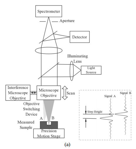
A white light interferometer is a low coherence interference microscope, a board spectral width light source and illumination lens is used to uniform illuminate the measured surface. A Mirau interference microscope objective lens is mounted on a piezoelectric transducer to scanning along the vertical direction. Light reflected from the measurement surface is imaged on the CCD array. The Mirau objective lens causes the same aberration to the reference beam and the measured beam, so it avoids additional phase error. The scanned interference image array records the signal envelop of the interference fringes from multiple wavelength, and the position of envelop marks the surface profile information in the field of view. However, when it comes to the situation of one layer of transparent film coated on an opaque surface, there are at least three readily identifiable envelop signal components, corresponding to the top surface, the substrate surface, and an echo resulting from the internal reflection. In our prior practice, thin transparent films and structures are more complex in product wafers, thus a theoretic model is impossible to handle inline metrology.
To address this bottleneck, a spectrometer which measures spectrum with high precision at the reference location of the test surface was added to a typical WLI optical system, as illustrated in Figure 1(a). Different from traditional spectral reflectance signal, the reflectance is modulated by the interference optical path difference since the spectrometer share the interference object lens. The optical path difference (OPD) is considered as an additional thickness parameter. The thickness of transparent films can be estimated [4, 5]; through the introduction of compensation, the accuracy of surface profile result is improved. For VIA dishing measurement, because of the height differential between metal and dielectric, OPD between reflected object waves and reference waves are different outside or inside the VIA zone. A piezoelectric linear actuator drives the interference microscope objective scanning along the normal direction, and an array CCD sensor obtained a group of interference pattern images by superimposed wide band waves. The intensity signals received by each pixel are modulated by scanning OPD, they record the height information of surface and layers. So the surface profile can be resolved form the interference image arrays.
To address this bottleneck, a spectrometer which measures spectrum with high precision at the reference location of the test surface was added to a typical WLI optical system, as illustrated in Figure 1(a). Different from traditional spectral reflectance signal, the reflectance is modulated by the interference optical path difference since the spectrometer share the interference object lens. The optical path difference (OPD) is considered as an additional thickness parameter. The thickness of transparent films can be estimated [4, 5]; through the introduction of compensation, the accuracy of surface profile result is improved. For VIA dishing measurement, because of the height differential between metal and dielectric, OPD between reflected object waves and reference waves are different outside or inside the VIA zone. A piezoelectriclinear actuator drives the interference microscope objective scanning along the normal direction, and an array CCD sensor obtained a group of interference pattern images by superimposed wide band waves. The intensity signals received by each pixel are modulated by scanning OPD, they record the height information of surface and layers. So the surface profile can be resolved form the interference image arrays.


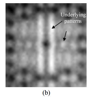
  Figure 1. (a) Illustration of WLI system structure with an additional spectrometer; (b) Intensity image of one frame from original WLI dishing measurement shows underlying structure.
Generally, due to the surface interference signal is suffered fromdegenerationcaused by the complicate sub-layer signal. As shown in Figure 1(b), the isolated dark spot is the desired target for CMP process control. But in practical measurement, its signal is interfered by underlying structure’s signal, causing errors to phase shifting solution. Also, step height characterization cannot be directly conducted because height information lacks absolute verification in traditional WLI measurement when involving transparent films.
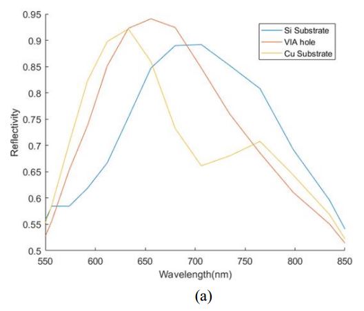
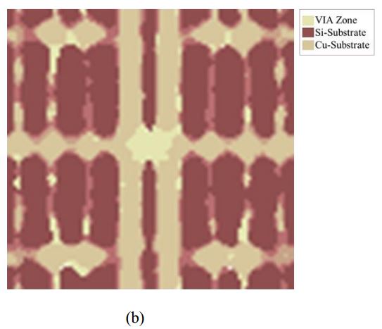
By referring to spectrum data, pixels in the field of view are segmented to several zones. For example, the VIA zone, Si-substrate zone with low under layer reflectivity, and Cu-substrate zone with high under layer reflectivity are 
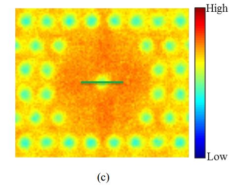
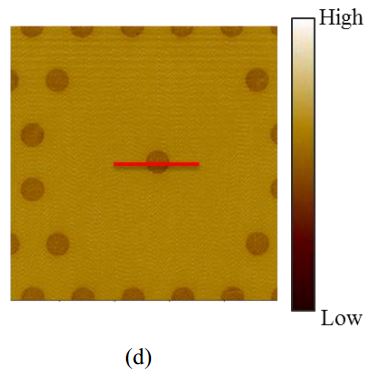
distinguished, as shown in Figure 2(a). With the classification model, every pixel in the field of view is classified into three categories, forming a zone map basically contains surface, film and structure information, which can be further verified by multi-layer pattern designs. Furthermore, height derived from each category has stable offset to each other, then a following calibration step will be performed to determine the offset values and feed them to equipment’s automatic data output system. The height calibration can be readily performed by high-accuracy AFM measurement. Figure 2(c) is the calibrated height image with the reference AFM data Figure 2(d), which provides VIA-Si substrate and VIA-Cu substrate offsets integrated into metrology recipe settings. After adding a fast spectrum collection and classification, WLI is thereby enabled on measuring patterned samples coated with transparent dielectric films.


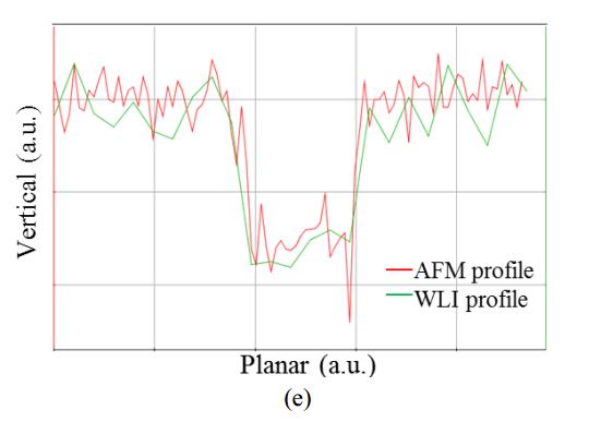
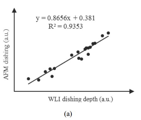
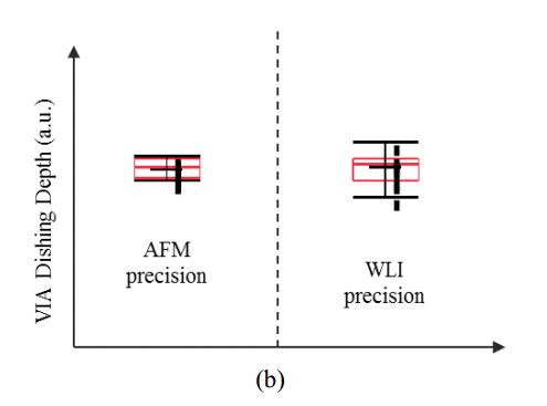
  Figure 2. (a) Three typical spectra type collected by spectrometer for classification; (b) Zone map of pixel classification based on spectrum; (c) Calibrated height image with the reference of (d) AFM measurement by comparing the relative height offset of each distinguished zone; (e) Target VIA data comparison of AFM and improved WLI.
3.   Image Processing for Better Resolution
Due to the via diameter is approaching the diffraction limit and dishing is far less than the wavelength, interference signal suffers noise and blurring. In order to solve these problems, the original data acquired by the sensors is processed by an automatic integrated application. A series of image processing are applied for image restoration, noise will be suppressed and images are enhanced to a certain degree.
Interpolation combine sub-pixel method processing of WLI images are implemented, as shown in Figure 3. According to spectrum range of light source, interference pattern signal acquired by each pixel is processed by Frequency domain band pass filtering to reducelow and high frequency noise. For approaching diffraction limitation, frequencydomain deconvolution by Wiener filter is used to enhance the side walls profile. The pixels inside and outside the dishing can be distinguished. According to the confidence level of each pixel acquiredbycalculat e the bias after processing, dependable pixel values are selected to calculate the output result. Image registration is applied to eliminate the alignment error of the measurement location. Edge detection extract the significantly feature; exclude the influence of light intensity. The phase correlation method uses the fast Fourier transform to compute the rotation and translation with sub-pixel accuracy between the different measured images. It ensures that the measuring points are consistent.


Figure 3.   Signal processing flow chart.
4.   Results and Discussion
Since WLI monitor dishing depth is not a traditional metrology method, a correlation study between WLI and AFM was done by measuring the same target VIAs in different shots one a 12-inches wafer. After the subpixel precision pattern recognition and image processing algorithms applied, the WLI precise of the micron or sub-micron VIAs is comparable with AFM. The Figure 4(a) demonstrates the correlation of the WLI measurements to AFM measurements of dishing depth. The data was collected post metal CMP process; after the collection of WLI data, AFM data was collected immediately. The linear R2 of dishing depth data measured by WLI and AFM is 0.9353, and overall bias between two measurements is tiny.
Additionally, in order to monitor the inline product dishing depth, the WLI measured the dishing depth precision was conducted. Although mean value of height measurement is comparable, compared to AFM, the modified WLI method yields lower repeatability and reproducibility, shown in Figure 4(b), nearly twice worse. The major reason is still the optical diffract limitation that restricts the valid data amount. VIA size is a critical dimension, which is usually within micrometer to achieve higher memory density. Subpixel approaches cannot completely solve physical resolution limitation. Potential improvement includes applying wider range light source, applying advanced objective design etc.


  Figure 4. (a) Correlation of WLI measurements of VIAs dishing depth to AFM reference; (b) AFM and WLI measurement precision on VIA dishing metrology.
XtackingTM technology requests strict topography control due to wafer-to-wafer connection. VIA is crucial for electrical connectedness, while the globe flatness of wafer surface is also important higher yield and less process defects. The ultimate goal for us is to create a fast, accurate and short-cycling metrology for large area topography measurement. We will further investigate the feasibility of whole-chip and all-weather WLI metrology that related to 3D NAND fabrication.
5.   Conclusion
In this paper, we demonstrated a method of measuring VIA dishing depth by white light interference WLI. After the subpixel precision pattern recognition and image processing algorithms processes, WLI is capable to replace AFM in dishing depth measurement. This method offers some main advantages over the traditional method like non-contact optical measurement and high throughput. High accuracy and acceptable precision was achieved in ultra-fine VIA dishing measurement. This work may shed light to future WLI applications and advanced optical process control methods.
Acknowledgments
We thank Park Systems for AFM equipment (NX-Wafer) support and continuous improvement..
[1] Simon Yang, "Unleashing 3D NAND's Potential with an Innovative Architecture," Keynote Speech, Flash Memory Summit, Santa Clara, CA, USA, August 7, 2018.
[2] Sicong Wang, Jian Mi, Abhishek Vikram, Gao Xu, Guojie Chen, Liming Zhang, Pan Liu, "Novel pattern-centric solution for high performance 3D NAND VIA dishing metrology", Design-Process-Technology Co-optimization for Manufacturability XIII, Proc. of SPIE Vol. 10962-42, (2019).
[3] Chen, Jianchao. "Comparison of optical surface roughness measured by stylus profiler, AFM, and white light interferometer using power spectral density." Proc Spie 7656.2(2010).
[4] P. de Groot, "Interference microscopy for surface structure analysis," in Handbook of Optical Metrology: Principles and Applications, T Yoshizawa, Ed., Boca Raton: CRC Press 797-809(2015)
[5] Kitagawa, Katsuichi. "Thin film thickness profile measurement using an interferometric surface profiler." Optomechatronic Sensors & Instrumentation III International Society for Optics and Photonics, 2007.
Article and author information
Xiaoye Ding
Sicong Wang
Yi Zhou
Yanzhong Ma
Le Yang
Chi Chen
Publication records
Published: Dec. 25, 2019 (Versions2
References
Journal of Microelectronic Manufacturing