Research Article Archive Versions 1 Vol 2 (4) : 19020409 2019
Download
Current Status of the Integrated Circuit Industry in China Packaging and Testing Industry Review
: 2019 - 10 - 16
: 2019 - 12 - 30
2105 41 0
Abstract & Keywords
Abstract: China's IC industry has been flourishing in recent years, huge market demand together with government investments are the major driving forces for this development. The status and development momentum of the Chinese IC industry also attracted wide interest and attention of international counterparts. A group of domestic IC experts are invited by the JoMM to write a series of articles about China's IC industry, including the history, current status, development, and related government policies. Information in these articles is all from public data from recent years. The purpose of these articles is to enhance mutual understanding between the Chinese domestic IC industry and international IC ecosystem. The following article is the third one of this series, the status quo of China's IC industry. The IC industry chain is very long including design, manufacturing, special equipment, materials, packaging and testing. The article series are arranged in accordance with this scope.
Keywords: Packaging; Testing Industry
1.   Situation of Packaging and Testing Industry
1.1.   Domestic Status of Packaging Industry
The integrated circuit (IC) industry chain mainly consists of three parts: design, manufacturing, packaging and testing. Packaging and testing is an important part of the semiconductor manufacturing process. Specifically, packaging is a process that protects the chip from physical, chemical and other environmental damages. It also connects the I/O port of the chip to a printed circuit board (PCB) glass substrate to achieve electrical connection and ensure normal circuit operation. Testing mainly focuses on the function and performance test of chips, circuits and aging circuit products.
It is urgent to find another way to continue technological progress since Moore's Law is limited by physical limits and huge capital investment. With advanced packaging integration technology, it is easier to achieve high-density integration, miniaturization and lower cost. The packaging industry will play a more important role in the integrated circuits, and it will also affect the industry more. With the development of advanced packaging, the integrated circuit industry will show some new trends.
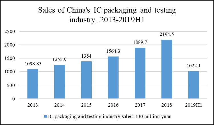
At present, China's IC packaging has sound policy support under the background of China's industrial upgrade. At the same time, the rise of China's consumer electronics industry and the increasing number of engineers in related industries have led to the rapid development of China's IC packaging industry. In 2012, the revenue of China's IC packaging and testing industry was only 80.568 billion yuan, and in 2016 it increased to 152.32 billion yuan, which is 1.89 times of 2012. In 2018, the sales revenue of the IC packaging and testing industry was 219.39 billion yuan, accounting for 33.6% of the total industrial value. In the first half of 2019, the sales of China's integrated circuit packaging and testing industry was 102.21 billion yuan, a year-on-year increase of 5.4%, as shown in Figure 1. ASIACHEM Consulting predicts that China's semiconductor packaging and testing market (including IDM) will exceed 400 billion yuan by 2023.


Figure 1.   Sales of IC packaging and testing industry from 2013 to the first half of 2019.
Through mergers and acquisitions, the high-end development of China's packaging and testing industry has completed domestic technical replacement, and has become the most competitive link in the industry chain. Based on the advantages of cost and consumer market, global semiconductor manufacturers have moved packaging and testing factories to China in recent years. A variety of domestic packaging and testing companies have already mastered the most advanced technology, and have gradually narrowed the technology gap with leading companies. At present, the domestic packaging and testing industry is supported by sole foreign investment, Chinese-foreign joint venture and domestic investment. Through overseas acquisitions, mergers and reorganization, JCET, TSHT, TFME and other domestic enterprises have constantly participated in international competition and their advanced packaging capacity has been greatly improved. Now they have entered the top 20 global packaging and testing companies.
1.2.   Regional Analysis of Domestic Packaging Industry
The packaging industry is downstream of the integrated circuit industry chain. At present, the domestic packaging and testing industry has already been in the world's first echelon. From 2016 to 2019, the industry of packaging and testing has maintained a growth rate of more than 15%. Compared with IC design and wafer manufacturing, the packaging and testing industry has lots of advantages such as less investment and fast construction speed. With the advantages of cost and geography, the semiconductor packaging and testing industry has been rapidly developed in China in recent years. In addition, a variety of semiconductor packaging and testing companies have emerged in China.
From the perspective of regional characteristics, the industrial clustering distribution of China's integrated circuit packaging equipment and materials market has further emerged, and an industrial space pattern has been formed that is concentrated in the three core areas of the Yangtze River Delta, the Bohai Rim, and the Pearl River Delta. The areas of the Yangtze River Delta, the Beijing-Tianjin-Bohai Rim, the central and western regions, and the Pearl River Delta respectively account for 56.2%, 14.6%, 12.4%, and 12.4%, and other regions accounted for 4.4%. Specifically, Shanghai, Jiangsu and Zhejiang's Yangtze River Delta area is the most important integrated circuit development and production base in China. A relatively complete integrated circuit industry chain including research and development, design, chip manufacturing, packaging and testing, and support industries has been initially formed in the Yangtze River Delta region. 55% of domestic integrated network manufacturing companies, 80% of packaging equipment companies, and nearly 50% of packaging material companies are located in the region. In the Bohai Rim region, Beijing, Tianjin, Hebei, Liaoning and Shandong provinces and cities have also become an important integrated circuit research and development, design and manufacturing base in China. The region has basically formed an entire industry chain of design, manufacturing, packaging, testing, equipment and material, thus has the conditions for mutual support and cooperative development. The Pearl River Delta region is also an important domestic electronics manufacturing base and main integrated circuit device market. In this area, the demand for integrated circuits has always accounted for more than 40% of the whole industry. Relying on the developed electronics manufacturing industry, IC packaging equipment industry in the region has developed rapidly in recent years.
1.3.   The Gap between the Domestic and Foreign Packaging Industries
In China's IC packaging market, traditional packaging such as DIP, QFP, QFN, DFN still dominates the market, accounting for more than 70% of the packaging market share. However, advanced packaging such as BGA, CSP, WLCSP, 3D stacking only account for about 20%. In recent years, JCET, Tongfu Microelectronics, Tianshui Huatian Technology and other companies have gradually approached or even surpassed international advanced levels in the field of surface mount area array packaging, relying on their own technical advantages and the support of major national science and technology projects.
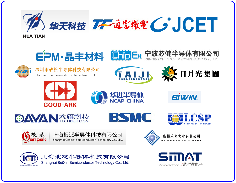
As shown in Figure 2, China's packaging companies are divided into three levels according to the maturity of advanced packaging technology.
The first level is innovative packaging technology companies. The main products of these large-scale leading enterprises include BGA, CSP, WLCSP, Flip-Chip, MEMS, Bumping, TSV, etc. Meanwhile, some domestic-funded enterprises are still focusing on DIP and SOP products.
The second level is packaging technology application companies that focus on technology application and process innovation. These enterprises are of medium size and have certain technical strength. They mainly focus on TO, DIP, SOP, QFP, QFN, DFN, and are gradually transiting to produce BGA, CSP, TSV and other advanced products.
The third level is small scale companies. They are weak at technology or production management, and mainly focus on traditional products such as TO, DIP, and SOT.


Figure 2.   Major integrated circuit packaging and testing companies in China.
2.   Introduction of Domestic Packaging and Testing Companies
2.1.   JCET Group Co., Ltd
On December 23, 2014, the world's fourth largest packaging and testing company, Singapore's STATS ChipPAC Ltd was acquired by JCET , making JCET enter the first level of global semiconductor packaging and testing. In 2016, JCET became the third largest packaging and testing company in the world, with a market share of up to 10%. Its packaging business covers solutions from discrete devices, wire bonding and flip-chip packaging to advanced wafer level packaging (WLP), Package-on-Package (PoP) and system-in-package (SiP), with advanced substrates for SiP, High-end encapsulation, high-density SMT and electromagnetic shielding processes. Its testing business provides test platforms and technical services, supporting communications, consumer and computer-based semiconductor chips, mainly including mixed-signal, RF, logic and high-performance digital chips. Also, comprehensive testing services including wafer testing, RF testing, product testing, and system-level testing, provides a wide range of test such as RF, analog, mixed-signal, digital, advanced digital circuits, and memory.
2.2.   Tianshui Huatian Technology Co., Ltd
Founded on December 25, 2003, TSHT mainly engages in semiconductor integrated circuit packaging and testing business. The packaging products mainly include DIP/SDIP, SOT, SOP, SSOP, TSSOP/ETSSOP, QFP/LQFP/TQFP, QFN/DFN, BGA/LGA, FC, MCM (MCP), SiP, WLP, TSV, Bumping, MEMS and other series. These products are mainly applied to computers, network communications, consumer electronics and intelligent mobile terminals, the IoT, industrial automation control, automotive electronics and other intelligent electronic fields. The company is actively committed to the development of high-end packaging technology for integrated circuits and the development of CSP packaging technology. The Xi'an base has begun to extend to packaging products such as SiP (system-in package), MEMS, FlipChip, CSP (chip-level package), and Laminate.
2.3.   Tongfu Microelectronics Co., Ltd
TFME was established in October 1997 and listed on the Shenzhen Stock Exchange in August 2007. TFME specializes in packaging and testing of integrated circuits. It is a national key high-tech enterprise, a vice-chairman unit of the China Semiconductor Industry Association, an executive vice-chairman unit of the National Integrated Circuits Packaging and Testing Industry Chain Technology Innovation Alliance, a top 100 Chinese electronic information company, China's top three integrated circuit packaging and testing companies.
In May 2016, TFME completed the acquisition of AMD Suzhou and Penang. TFME has advanced packaging and testing technologies such as bumping, WLCSP, FC, BGA, and SiP, traditional packaging and testing technologies such as QFN, QFP, SO, and wafer testing and system testing technology. TFME also apply their packaging and testing technologies in automotive electronics and MEMS. Meanwhile, the company is the first domestic enterprise to realize the full-scale large-scale production of 12-inch 28-nanometer mobile phone processor chips, including bumping, CP, FC, FT, SLT, etc. Its products and technologies are widely used in high-end processor chips (CPU, GPU), memory, information terminals, IoT, power modules, automotive electronics and other fields facing the intelligent era in the cloud, management, and end fields. More than half of the world's top ten semiconductor manufacturers are its customers.
2.4.   Wuxi China Resouces Micro-Assembly Technology Co., Ltd
Anst is a subsidiary of China Resources Microelectronics, a well-known national microelectronics company in China. It focuses on the design of integrated circuit packaging / test solutions for semiconductor chip design and wafer manufacturers at home and abroad foundry services. After years of development, Anst has developed more than ten series of packaging including DIP, SOP, SSOP, MSOP, QSOP, TSOT, QFP, QFN, FC, etc. And it focuses on providing professional packaging and testing services for Leaded Package and QFN Package integrated circuits for leading semiconductor design companies at home and abroad.
2.5.   ASE Technology Holding Co., Ltd
ASE is a global leader in semiconductor packaging and testing manufacturing services. It provides customers with integrated services including front-end engineering testing, wafer pin testing and back-end semiconductor packaging, substrate design and manufacturing, and products testing. Now the company's main packaging products have all entered the mass production stage, including flip chip packaging, wafer level packaging (CSP), stacked package (PoP), system in package (SiP), sensor packaging (MEMS and Sensor Packaging ), Fan-out packaging (Fan Out), 2.5D/3D IC packaging, green environmental protection packaging and 300mm rear section unified technology solutions.
2.6.   China Wafer Level CSP Co., Ltd
China Wafer Level CSP Co., Ltd is the first domestic company engaged in wafer-level chip packaging of image sensing chips (CCD and CMOS). Its wafer-level chip packaging technology is the only one in the world that can mass-produce large-scale production of image sensing chip applications, which has a market share of more than 40% in this field. The company has a strong industrial background and financial strength, and its funding consists of Israel and the most powerful domestic venture capital investment institutions. The Suzhou factory was put into production in early December 2005. On June 15, 2012, the company's listing was approved by the issuance review committee of the Securities and Futures Commission, and then the company issued an initial public offering of stock prospectus.
In 2018, the company took a series of actions for further development as follows. It continued to focus on advanced packaging business in the sensor field, and worked hard to extend its core components, modules, and test business. It oriented to the needs of the market and customers, adhere to the global layout of continuous technological innovation and intellectual property system, and promote the continuous upgrade and optimization of technologies and processes to adapt to market development and new needs in new areas and new products. It continued to increase 8 inches , 12-inch 3DTSV packaging technology process capacity and production scale level, consolidate and enhance the company's technological leadership and market size advantage in this field; continued to innovate biometric chip packaging technology, using its own technology and IP advantages. The module technology and integration capabilities of the acquired assets are engraved for innovation and effective integration, with diverse packaging technologies such as Trench, TSV, LGA and full solution service capabilities; actively developing high-end product fan-out packaging technology and system-level packaging, automotive electronics product packaging technology and other application development technology.
2.7.   Shenzhen Siga Semiconductor Technology Co., Ltd
Founded in 1997, Shenzhen SIGA is a modern national high-tech enterprise specializing in integrated circuit chip packaging, R&D, and production. Since its establishment, the company has been committed to the development of chip packaging and testing industries such as LED driver integrated circuits, power supplies, communications, storage, and photosensitive integrated circuits. The company has formed a professional team of semiconductor production technology management, relying on leading technology, advanced equipment, scientific management, product quality reaches international standards, and is well received by the semiconductor industry. At present, the company's main integrated circuit packaging products include DIP, SOP, TO and so on.
2.8.   Suzhou Good-Ark Electronics Co., Ltd
Good-Ark is a leading diode packaging company in China. The company's predecessor is Suzhou Gushen Electronics Co., Ltd., which is composed of Suzhou Tongbo Electronic Equipment Co., Ltd. Initiated by General Electric Co., Ltd. and Shanghai Huiyin (Group) Co., Ltd. It was reorganized to Suzhou Good-Ark Electronics Co., Ltd. in July 2002 and successfully listed on the Shenzhen Stock Exchange in November 2006.
The company is mainly engaged in diode chip manufacturing and diode packaging, testing, and sales. The main products include: 3 inch\4 inch wafers, 14 types of rectifier diodes such as glass passivated rectifier diodes, and 2 types of voltage regulators such as zener diodes, various high-speed switching diodes and silicon bidirectional trigger diodes. At present, the company's packaging products include DIP, SIP, SOP, TO, PLCC, DFN, LGA, MEMS, etc.
2.9.   Biwin Storage Technology Co., Ltd
Biwin is a group company engaging in integrate production and sales. The company's main products and services include SSD solid state disks, embedded storage chips, SIP modules, and packaging and testing services. It has a global market share of more than 20%. It has own branches in Taipei and the United States, and it was listed on the Shenzhen Stock Exchange in 2015.
Biwin's packaging electronics assembly workshop integrates Flash packaging, SSD production, and sales. It has its own FLASH packaging workshop (equipment investment amounted to 300 million yuan). Mass production of SSD is huge in China, with more than 500 employees. The brand products sold independently are SSD, qNAND (e-MMC), eSSD, cNAND, MCP; the company has advanced packaging manufacturing capabilities with SIP as its core, and has been deeply cultivating advanced packaging foundry field for nearly 20 years, and has accumulated rich technology experience and packaging process. At present, the company's main packaging products and services mainly consist of BAG, LGA, QFN, SIP, and TSOP.
2.10.   National Center for Advanced Packaging (NCAP China) Co., Ltd
NCAP China was formally registered in Wuxi New District in September 2012. Its main business is system-level packaging and advanced technology research and development. The company's research areas include 2.5D/3D TSV interconnect and integration key technologies, wafer-level high-density packaging technology, SiP product applications, and verification, improvement and research and development of materials and equipment related to packaging technology, providing system solutions for industry.
The company's R & D platform includes an advanced package design simulation platform, a 2200 square meter cleaning room and a 300mm (200mm compatible) advanced package R & D platforms (including 2.5D/3D IC back-end processes and micro-assembly), package substrate lines, testing laboratory and reliability and failure analysis platform. The company's main packaging product services currently include BGA, LGA, WLCSP, Bumping and 2.5D packaging.
2.11.   Shanghai Beixin Semiconductor Technology Co., Ltd
Shanghai Beixin Semiconductor Technology Co., Ltd. was founded in Zhangjiang High-Tech Park, Pudong, Shanghai in 2013. It has a variety of advanced packaging and testing equipment, analysis and verification equipment. Also it has formed an experienced working team. It provides fast and professional technical analysis and testing services such as chip packaging, reliability testing, FIB, competitiveness analysis, SEM, and CP testing. At present, the company's main packaging products and services include three types of fast plastic packaging, fast ceramic and COB packaging, fast BGA & LGA & MEMS packaging, covering QFN, DFN, SOP, TO, etc.
In addition, there are other companies engaging in packaging and testing business such as Taiji Semiconductor (SuZhou) Co., Ltd, Shanghai Genpek Semiconductor Technology Co., Ltd and Shanghai Simat Microelectronics Technology Co. Ltd, etc.
3.   Future Outlook and Suggestions
On one hand, with the increase of integrated circuits’ complexity, the increase in information per unit volume and the faster processing time per unit time, there is an increase in the number of pins of packaged products. On the other hand, with the miniaturization of electronic products, market puts forward corresponding requirements for circuit packaging technology, also the size and number of chips that can be carried in a unit volume should be valued more. In the industry, miniaturization of electronic products is a strong downstream demand, which will definitely drive the rapid development of advanced packaging technology. Those companies with advanced packaging technology will also have obvious market advantages.
3.1.   Changing Trends of Advanced Packaging in the Future
Overseas mergers and acquisitions in recent years have enabled domestic packaging and testing companies to quickly acquire technology and markets, which greatly promote the upward development of China's packaging and testing industry. However, due to the recent rigorous overseas audits that have hindered international investment and mergers and acquisitions and reduced optional M & A targets, China's future possibility of acquiring advanced packaging technology and market share through mergers and acquisitions will decrease. Independent R&D and domestic integration will become the mainstream.
Referring to independent R&D, as advanced packaging involves resources such as technology types and equipment used in wafer manufacturing, packaging foundries may choose to cooperate with wafer manufacturing foundries under technical or financial constraints, or in the form of technology licensing cooperating with the huge production capacity of packaging and testing foundries for orders and mass production, and jointly expand the market. According to the current process of domestic wafer manufacturing foundries, the cooperation direction is mainly wafer-level packaging and low-density integration, and there is still a long way to go in the research and development of high-density integration.
In addition, with the increase of the technology complexity and the capital investment, fewer companies can follow the development of advanced packaging technology. If smaller packaging and testing manufacturers are unable to occupy the niche market, their competitiveness will decline, which may trigger new mergers and acquisitions, and further increase the concentration of the market.
3.2.   Speed up the Construction of Virtual IDM Ecological Chain
In recent years, China's integrated circuit packaging and testing industry has achieved rapid development and great progress. However, the overall technical level of the domestic integrated circuit packaging and testing industry is still not strong enough. In recent years, much attention has been paid to the integrated circuit industry, and it is necessary to promote the development of advanced packaging industry. In China, packaging and testing industry is the earliest developed industry of the three integrated circuit industries (design, manufacturing, packaging and testing). At present, the industry will be well developed since the gap with the international level is relatively small.
It is imperative to promote the construction of the virtual IDM ecological chain of the integrated circuit industry chain of “EDA software—chip design—chip manufacturing—chip packaging and testing—whole machine application” in China. It is imperative that the rapid development of China's integrated circuit packaging and testing industry will be driven by market demand. The competition of integrated circuits will eventually manifest as the competition of comprehensive strength between industrial chains, and the development of advanced packaging requires the coordination of processes, equipment and materials. In the new technology trend and competitive environment, the integrated circuit industry is increasingly showing competition for the overall strength of the industry chain. Over the past few years, international semiconductor manufacturing companies have stepped up their efforts to advanced processes. Driven by continued large-scale capital investment and expansion of production capacity, some major semiconductor manufacturing companies also have complete advanced packaging manufacturing capabilities.
In response to such an industrial situation, the key point is to break through some key technologies, such as high-density packaging, three-dimensional packaging, multifunctional chip stacking integration, and system-level packaging. It is necessary to construct a virtual IDM industry chain based on applications, transformation, multi-function, and a high starting point, to solve key technologies in the integrated circuit industry and break through technical bottleneck.
3.3.   Be Patient in the Packaging and Testing Industry
In recent years, domestic packaging companies have gradually grown up through acquisitions. However, it is widely criticized since their dissatisfactory performance after acquisition. For instant, the JCET’s risking acquisition of Singapore's STATS ChipPAC Ltd. in 2014 has been criticized since the "snake swallow elephant" merger making the company stuck.
In order to successfully implement mergers and acquisitions, JCET has paid a high price, but this is also the step that Chinese packaging companies must take when moving towards high-end. Judging from the current global semiconductor packaging industry trend, advanced packaging has become irreversible. Even semiconductor giants such as Intel, Samsung and TSMC have significantly increased their investment in advanced packaging. Advanced packaging represented by technologies such as flip chip (FC) structural packaging, wafer level packaging (WLP), system in packaging (SiP), 2.5D packaging, 3D packaging, etc., has accounted for more than half of the entire packaging market size, and it is also the main source of profit for packaging companies.
Although packaging and testing is the earliest developed part of China's integrated circuit industry, it is still dominated by the low-end market. If domestic packaging companies want to enter the high-end market and get further development, M & A is a feasible path although the company's profit will be affected for a period of time. However, the transformation and upgrading of an enterprise cannot be accomplished overnight. Based on this, the company needs to launch a series of time-consuming changes. It is hoped that the external industry can give companies a certain degree of tolerance, and that the packaging and testing industry must be strategically scheduled to become stronger.
Article and author information
Litho World
Publication records
Published: Dec. 30, 2019 (Versions1
References
Journal of Microelectronic Manufacturing