Research Article Archive Versions 1 Vol 3 (1) : 20030101 2020
Download
DFM: “Design for Manufacturing” or “Design Friendly Manufacturing”
: 2019 - 11 - 20
: 2020 - 03 - 18
: 2020 - 03 - 30
2822 83 0
Abstract & Keywords
Abstract: As the IC manufacturing enter sub 20nm tech nodes, DFM become more and more important to make sure more stable yield and lower cost. However, by introducing newly designed hardware (1980i etc.) process chemical (NTD) and Control Algorithm (Focus APC) into the mature tech nodes such as 14nm/12nm, more process window and less process variations are expected for latecomer wafer fabs (Tier-2/3 companies) who just started the competition with Tier-1 companies. With improved weapons, latecomer companies are able to review their DFM strategy one more time to see whether the benefit from hardware/process/control algorithm improvement can be shared with designers. In this paper, we use OPC simulation tools from different EDA suppliers to see the feasibility of transferring the benefits of hardware/process/control algorithm improvement to more relaxed design limitation through source mask optimization (SMO): 1) Better hardware: scanner (better focus/exposure variation), CMP (intrafield topo), Mask CD variation (relaxed MEEF spec), etc. 2) New process: from positive tone development to negative tone development. 3) Better control schemes: holistic focus feedback, feedback/forward overlay control, high order CD uniformity improvement. Simulations show all those gains in hardware and process can be transferred into more relaxed design such as sub design rule structure process window include forbidden pitches (1D) and smaller E2E gaps (2D weak points).
Keywords: Design for Manufacturing (DFM); Design Friendly Manufacturing; EUV Lithography; Source Mask Optimization (SMO); Design Technology Co-optimization (DTCO); Process Window; Process Variation
1.   Introduction
1.1 Technology Revolution vs. Evolution
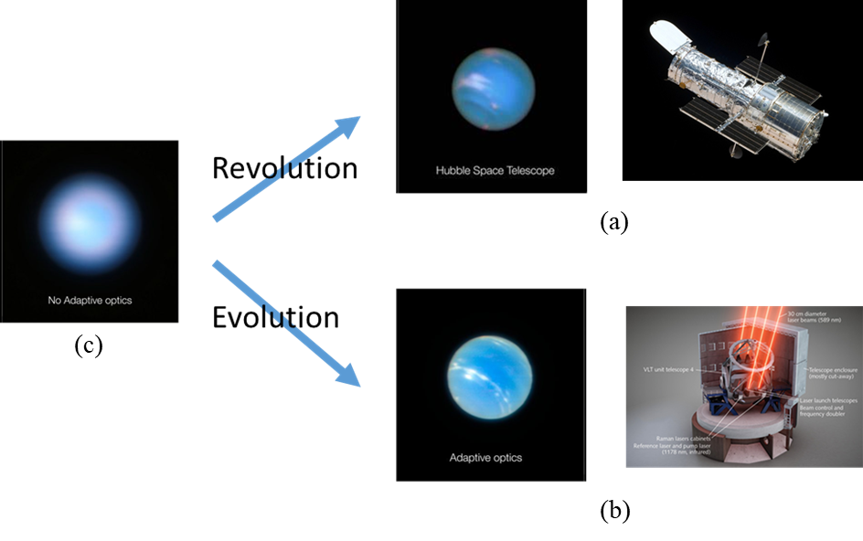
Since 1800, in the path of technology development, there were always a lot of revolutionary breakthroughs and small step evolutions. For example: in 1990, the Hubble Space Telescope(HST) Figure 1.a gave us a crystal-clear image of Neptune which surpass all the images taken before by earth based telescope (Figure 1.c). It is really a revolution technology breakthrough at that time. However, astronomers and engineers never stop exploring new technologies. Steps by steps, adaptive optics technology evolved with computer technology and laser technology development, gave world another wow image in 2017 by ESO (European Southern Observatory)’s VLT (Very Large Telescope) equipped with MUSE and GALILIA adaptive optics as Figure 1.b shown. Therefore, both revolution and evolution can help us arrive at same goal. In Photolithography, the same story kept happening: immersion lithography and EUV lithography are so called revolution technologies while OPC, illumination, mask, APC/AEC are evolution technologies. After a big leap with revolution technology breakthrough such as immersion and EUV lithography, different kind of evolution technologies jump into the battle to squeeze last drop of the juice from the new technology to make low k1 patterning possible.


Figure 1.   (a) Image of Neptune by HST (Hubble Space Telescope) 1999, (b) Image of Neptune taken by VLT (Very Large Telescope) 2017 with adaptive optics, (c) Neptune image taken without adaptive optics.
1.2 Revolution and Evolution in Low k1 Imaging


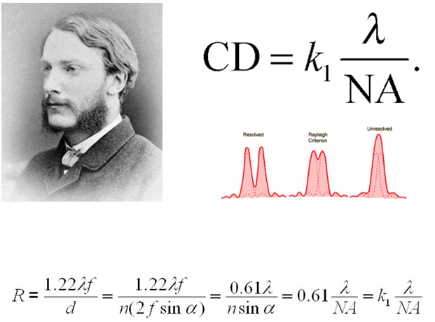
Figure 2.   Rayleigh Resolution Equation
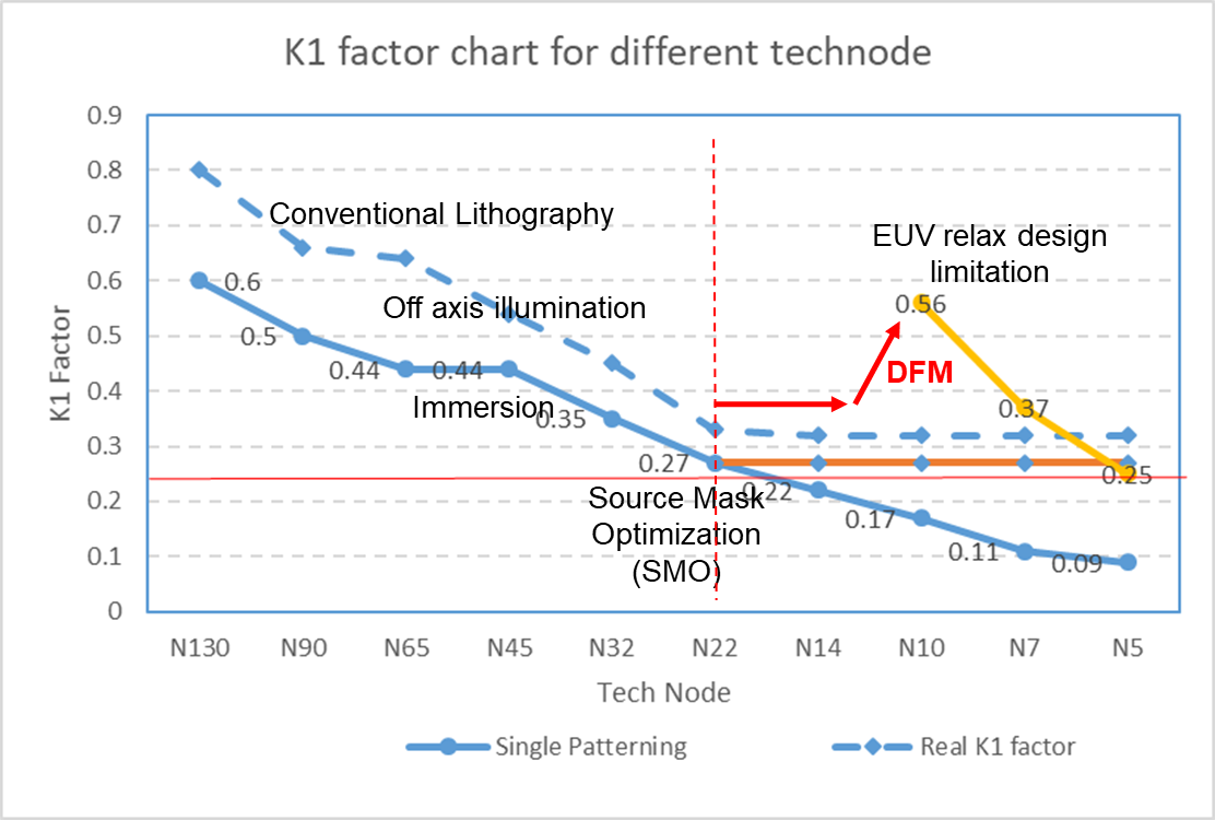
Rayleigh Resolution Equation (Figure 2) is a well-known equation to define the difficulty of the patterning process. The lower the k1 value the more difficult the patterning is. As a thumb of rule, k1~0.25 is the lowest value for single exposure patterning. However, k1 value is not a fixed value as the technology evolving. The manufacturable printability is actually the balance between process windows and process variations. For example, 60nm DOF@5%EL is very common process window criteria for sub 20nm tech node, but this criterion is just estimated based on inline focus variation 3sigma ~ 30nm and exposure (CD related variation) 3sigma~1mj/cm2. However, this process window criterion is not fixed though the technology evolution. Better hardware design, new photolithography chemical, new mask technology, advanced data analysis, OPC and AI control technologies all significantly reduced process variation (EPE variation), relatively process window become larger and result in higher k1 value. As Figure 3 shows, the solid blue line is the k1 factor when new tech node just released in R&D phase for Tier 1 Fab, the k1 value kept decreasing as the CD spec/design rule shrunk. And the dash line is the k1 factor in consequential years after patterning technology become mature when Tier-2/3 Fab jump in. With better hardware/process variation, the k1 value become larger compared with Tier-1 Fab as Tier-2/3 Fab move to mass production.


Figure 3.   k1 value trend chart with technology evolution and revolution.
However, before N22 tech node, such kind of k1 value improvement in Tier-2/3 Fab only reflected in better wafer yield and lower cost, the benefit never be shared with designer (because there is no significant design constraint when k1 value >0.3). When the technology entered sub 20nm node, not all the features can meet k1>0.25 criterion, so some feature types (such as forbidden pitches, special orientation or 2D structures) are sacrificed to make sure enough process window for the rest feature types through source mask optimization (SMO) methodology. The approach is called Design for Manufacturing (DFM), which put a lot of constraint on designer’s freedom and make IC design more difficult and limit the chip performance as well. Because of this constraint, EUV technology was pushed very hard to manufacturing after 14nm tech node. In Figure 3 solid yellow line shows, when 0.33NA EUV scanner released for N7 tech node, the k1 value jumped to as high as 0.56 which is at same level as 130nm tech node, design constraints are completely removed with single exposure and less process complexity, therefore we call EUV lithography as “Design Friendly Manufacturing” (DFM). It is very obvious to see Design Friendly Manufacturing concept can be applied when k1 increase. Later we will show, how SMO methodology can be used to apply Design Friendly Manufacturing concept in 14nm tech node as the process/hardware become more mature for Tier-2/3 Fabs than 7-8 years ago.
1.3 Source Mask Optimization (SMO) = Design for Manufacturing
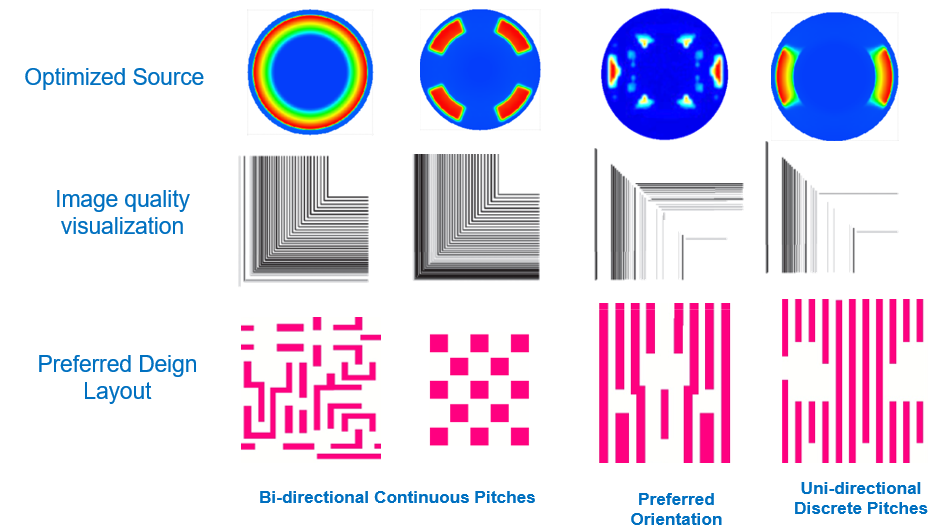
Source Mask Optimization (SMO) is a computational lithography methodology introduced in 2001 by Alan E. et al. from IBM [2] to customize the imaging light source shape to enhance process window for certain features defined by constrained design rule. As Figure 4 shows different illuminations are purposely customized for different designs: Annular illumination in general can support all type of features, but at cost of lower image contrast which is not much deal for large pitch design. On another extreme side, dipole illumination is only designed for line/space features with very limited pitch range and single orientation. In between those two extreme cases, quasar and free form SMO are generally designed to balance design limitation and common process window. As thumb of rule, the smaller illumination pixel cluster area (coherence of light), the more constraint on design and gain more process window for a small range of pitches by sacrificing the rest. Due to the constraint applied on design by SMO, it is generally called Design for Manufacturing (DFM) methodology, which need a lot of support from designers to co-work with Fab engineers to deliver manufacturable patterning solution.


Figure 4.   Through pitch printability of different illuminations (gray level of the 2nd row pattern indicates the printability of feature with different pitches and orientation. Black= largest process window, dark grey = reasonable process window, light grey = small process window and white = no process window). Source: “Design Technology Co-Optimization in the Era of Sub-Resolution IC Scaling” Lars W. Liebmann.
Term “Design for Manufacturing” (DFM) is as old as terms “forbidden pitch” and “off axis illumination” in microlithography industry, but it is more popularly mentioned as “source mask technology” SMO is widely used after sub 20nm when optical lithography approached k1~ 0.25, with a lot of design constraints are applied with aggressive source customization to gain process margin by sacrificing some designs. And multiple patterning technology further applies more constraint on design and increase design complexity as well, that is why EUV lithography was pushed to manufacturing after decades of struggling with tons of technical obstacles. The most important benefit from EUV lithography is it significantly relax the design limitation and make design much easier.
1.4 EUV = Design Friendly Manufacturing
EUV lithography was first mentioned as early as 1977. However due to tons of technical obstacles such as light source power, photoresist, mask blank defect etc., this technology has been delayed to mass production again and again until 2018, TSMC and Samsung announced their 7nm process with EUV solution [3, 4].
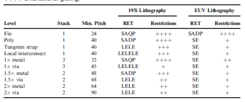
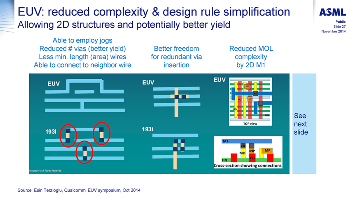
Compared with traditional immersion lithography, EUV lithography is high k1 lithography which means higher print fidelity, single exposure, less layers, less OPC and most important: less restriction on design. As following table shown from Liebmann et al. for 7nm, 193nm immersion not only need very aggressive RET method but also apply more aggressive design restriction to maintain same manufacturability as EUV lithography. And Figure 5 shows more detailed design limitation difference between 193nm immersion and EUV lithography: more 2D patterning freedom with single exposure, more freedom for redundant via insertion and significantly reduced MOEL complexity by EUV lithography. That is why we called EUV lithography as “Design Friendly Manufacturing” DFM.


Table 1   Patterning Solutions 193i vs. EUV. (Source: “Design Technology Co-Optimization in the Era of Sub-Resolution IC Scaling” Lars W. Liebmann)


Figure 5.   Design benefits from EUV lithography.
2.   From DFM to DFM
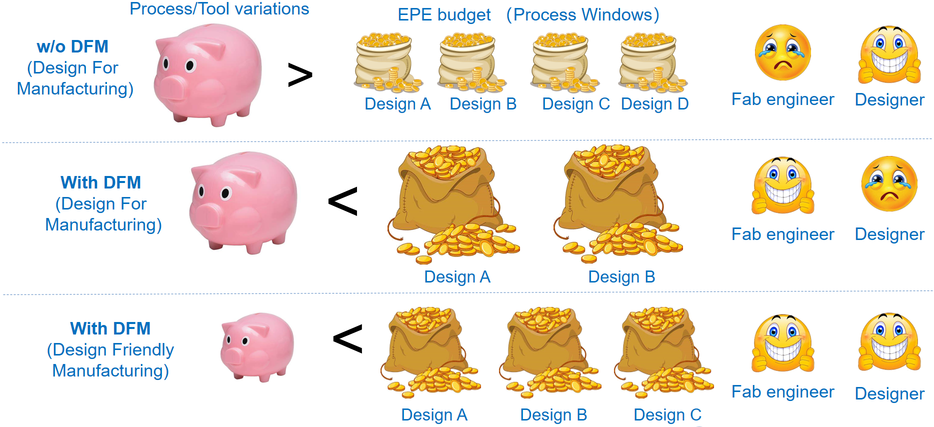
So with concept of Design Friendly Manufacturing borrowed from EUV lithography, we can do the same thing with evolutionary improvement in process/hardware variations. As mentioned in section 1: k1 value is actually the balance result between process window and process variations. Continuous process/hardware variation improvement effectively increase the k1 value with technology evolution. Same as EUV lithography, higher k1 value can also help to relax design constraint we have applied during lower k1 period. As following cartoon Figure 6 shows: at low k1 imaging era, without DFM (Design for Manufacturing) approach applied, all the allowed feature designs suffer smaller process window (less number of gold coin) compared with inline process/tool variation (size of piggy bank), Fab engineer suffered a lot while designer’s life is much easier. Then DFM method was applied to exclude certain process window limited structures from design rule, and the rest of patterns gain more window through SMO approach, so Fab engineer will be happy with better process windows (more gold coins than size of piggy bank) for yield improvement but designer is unhappy at all. With continuous process and hardware variation improvement, the size of piggy bank decreased until the number of coins are more than enough to fill the piggy bank, then we can include more design (coin bag) and rebalance the number of coins in each design (bag size) to make sure coins in each bag are enough to fill up the piggy bank. Therefore, with more design freedom and manufacturability maintained, both Fab engineers and design will be happier.


Figure 6.   How DFM (Design for Manufacturing) evolved to DFM (Design Friendly Manufacturing).
3.   Case Studies
3.1.   Negative Tone Development
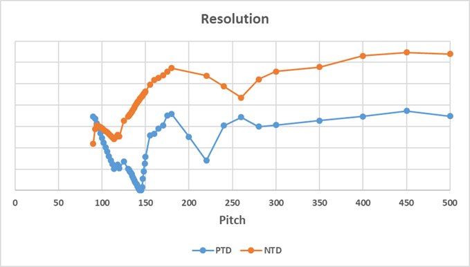
Negative Tone Imaging was first introduced by Tim Brunner IBM and Chris Mack [5, 6], in their papers it was shown with image tone switched it is possible to gain more process margin by tuning different print bias. As Figure 7 shows the image contrast of line/space is significantly improved by negative tone imaging at semi-dense and isolated trench structures.


Figure 7.   Through pitch image contrast for PTD and NTD process.
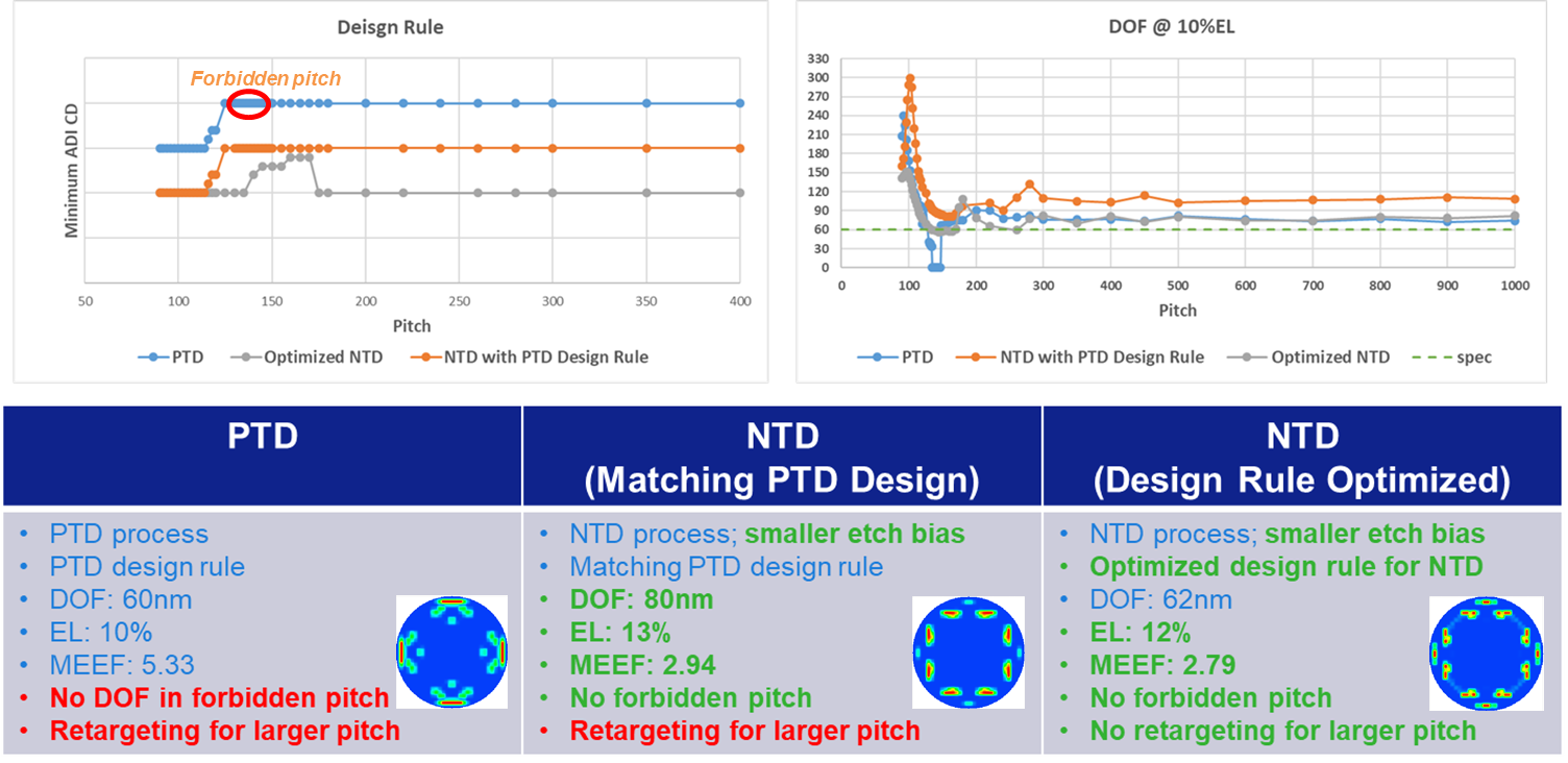
First of all, as our baseline, a lot of design constraints are applied in PTD process, especially for the forbidden pitches, and for semi-dense and isolated structures need retargeting to gain more process window as well (Figure 8). Then NTD process was introduced with new source but keep design constraint same as PTD process. With NTD process, both DOF and EL improved significantly semi-dense and isolated features (>80nm DOF is more than enough for 14nm BEOL), especially forbidden pitches. Furthermore, with design rule optimized (CD retargeting pitch reduced and include all forbidden pitches) with SMO fine-tuned, we can see more balanced process windows cross different pitches.


Figure 8.   Process window and design gains with NTD process by SMO fine-tuning for Metal layers.
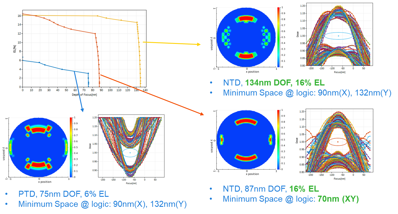
Same concept also applied on 14nm poly cut layers (short trench dominated layer). For this case, as Figure 9 shows NTD process show significant improvement is both common DOF and EL without design rule change. If we include more stringent design rule (minimum space in logic area from 90nm to 70nm) which is not printable for PTD process, with SMO fine-tuning, the common process window can be still maintained at 80nm DOF, the process window benefit from NTD has been shared with Fab and designers.


Figure 9.   Process window and design gains with NTD process by SMO fine-tuning for poly cut layers.
3.2.   Hardware/Process Improvement


Figure 10.   Process/Hardware variation improvement during the past years.
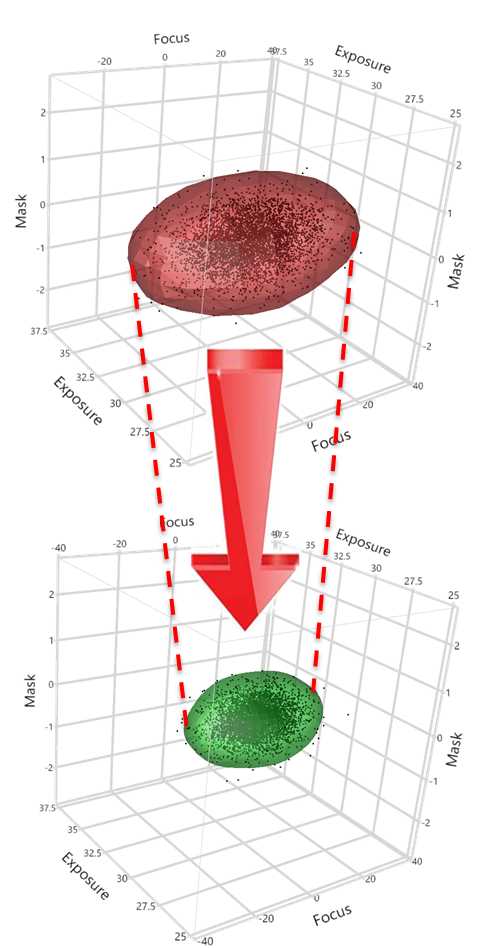
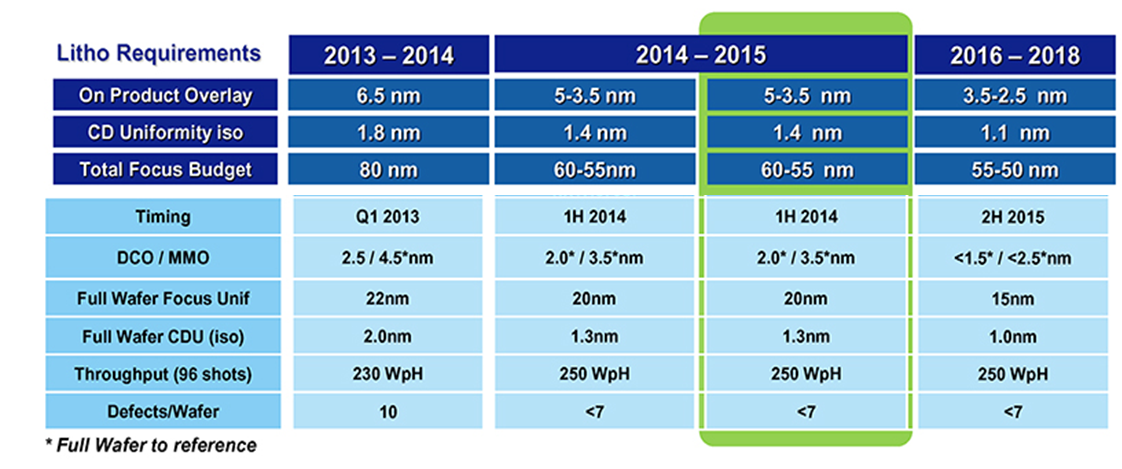
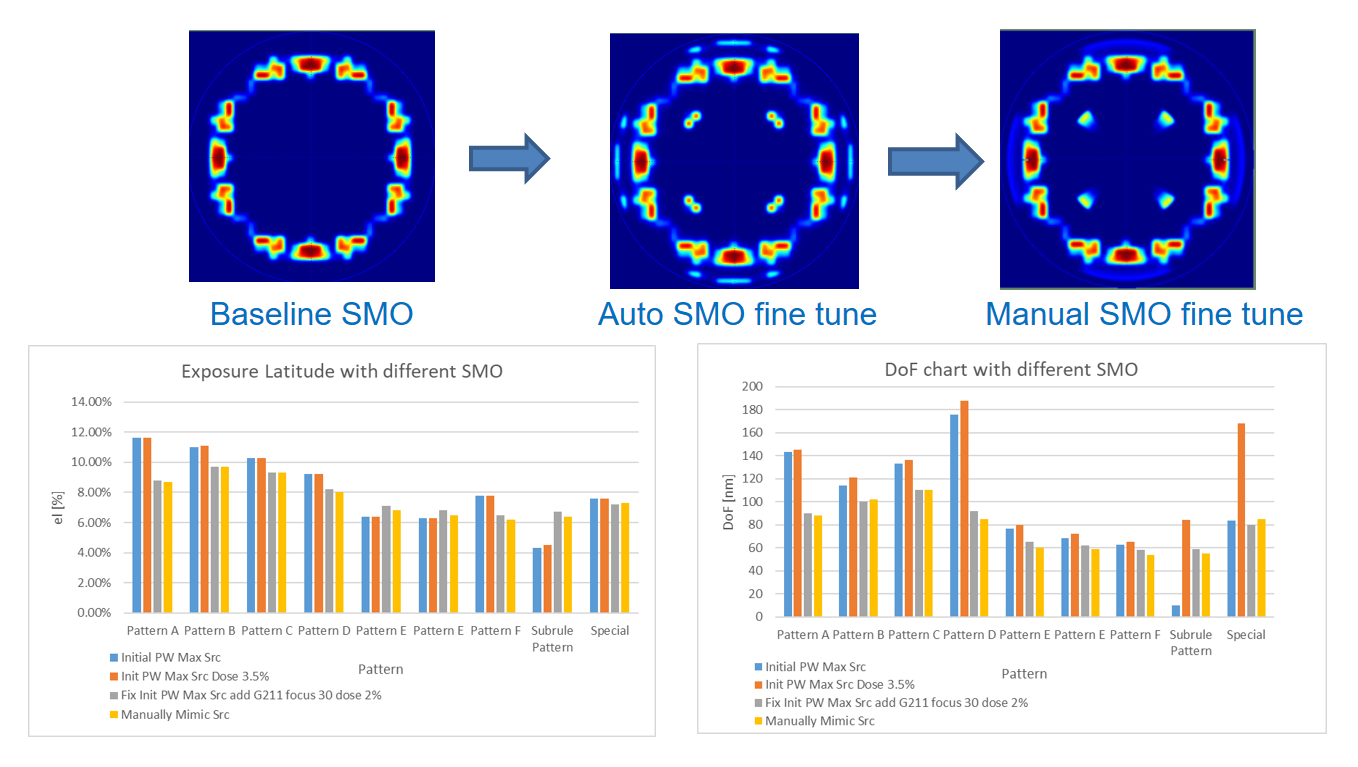
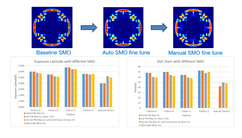
Besides new process change such as NTD, there are also a lot of hardware and process control improvement since 2013 when 16nm/14nm was first introduced into mass production. Figure 10 shows the lithographic uniformity improvement from 2013 to 2018, all EPE related uniformity improved by 30-40%, and real inline exposure/focus/mask variation 3D plot also show exposure/focus/mask CD variation improvement from 28nm to 14nm technode. And further improvement is still on-going with better APC (focus feedback control, integrated metrology CD/overlay, more accurate OPC, better CMP and etch in-coming control), another 10-20 % improvement can be expected. So let’s see what we can share with designer if process/hardware variation can be reduced compared process window. Figure 11 is the metal layer process first set up with criterial 60nm DOF @ 5% EL which was used as the standard criteria, gray bar is the process widow with baseline SMO, the DOF of sub-rule structure is so small that is not manufacturable with old DOF criteria. If we reduce the EL criteria to 3.5% only, the DOF jump to 80nm (orange bar) without any process change. That means sub pattern may not be manufacturable with old hardware/process but become printable with 30% process variation reduction. However, the process windows across different feature is not balanced at all. Then we need to fine tune the SMO to rebalance EL vs DOF cross different features. Both auto fine-tuned 2nd source and manual fine-tuned 3rd source shows the similar performance. Same thing happened on MEOL hole layer, as Figure 12 shown, the most significant improvement is the DOF of sub-rule patterns and SMO helps to rebalance between EL window and DOF window cross different structures.


Figure 11.   Process window and design gains with 40nm DOF@3.5%EL by SMO fine-tuning for metal layers.


Figure 12.   Process window and design gains with 40nm DOF@3.5%EL by SMO fine-tuning for hole layers.
4.   Conclusion
With “Design Friendly Manufacturing” concept borrowed from EUV lithography, we have used simulation (SMO) to explore the possibility of loose design limitation and increase design freedom with the help from evolutionary process/hardware stability improvement. And we also found the design benefit gained from SMO fine-tuning is feature type dependent and process dependent as well. For example, NTD process with SMO the design benefits are mainly forbidden pitch and selective CD retargeting while hole and short trench pattern with improved hardware variation is mainly impact on sub-rule design such as minimum space.
Next we will explore more detailed error budget such as MEEF and overlay to check the possibility of further optimization with real inline process variations and new RET approaches.
[1] ESO. "Supersharp images from new VLT adaptive optics." ScienceDaily, 18 July 2018;
[2] Alan E. Rosenbiutha, Scott Bukofsky et al. “Optimum Mask and Source Patterns to Print a Given Shape” Optical Microlithography XIV, Proceedings of SPIE Vol. 4346 (2001);
[3] “Samsung Says New 7-Nanometer Chip Production Starting This Year” May 23, 2018 Bloomberg;
[4] “TSMC Ready for EUV on 7, 5nm” May 3, 2018 EE times Asia;
[5] Chris A. Mack and James E. Connors "Fundamental differences between positive- and negative-tone imaging", Proc. SPIE 1674, Optical/Laser Microlithography V, (1 June 1992);
[6] Timothy A. Brunner and Carlos A. Fonseca "Optimum tone for various feature types: positive versus negative", Proc. SPIE 4345, Advances in Resist Technology and Processing XVIII, (24 August 2001);
Article and author information
Wenzhan Zhou
zhouwenzhan@hlmc.cn
Hung-Wen Chao
Yu Zhang
Chan-Yuan Hu
Wei Yuan
Yifei Lu
Hongmei Hu
Xiang Peng
Publication records
Published: March 30, 2020 (Versions1
References
Journal of Microelectronic Manufacturing