Research Article Archive Versions 1 Vol 4 (1) : 21040101 2021
Download
Recent Advances in Organic-inorganic Hybrid Photoresists
: 2021 - 02 - 11
: 2021 - 03 - 16
: 2021 - 03 - 28
1251 90 0
Abstract & Keywords
Abstract: Photoresists are radiation-sensitive materials used for forming patterns to build up IC devices. To date, most photoresists have been based on organic polymers, which have been dominating the semiconductor industries over the past few decades. It is obvious that extreme ultraviolet (EUV) lithography has become the next-generation lithography technology. The development of comprehensive performance EUV resist is one of the most critical issues. However, organic polymeric photoresists are difficult to meet the harsh requirements of EUV lithography. Pure inorganic photoresists such as metal salts, hydrogen silsesquioxane (HSQ) are expected for EUV lithography due to their high resistance and high resolution. But the low sensitivity makes them not suitable for high volume manufacturing (HVM). Organic-inorganic hybrid photoresists, containing both organic and inorganic components, are regarded as one of the most promising EUV resists. They combine both merits of organic and inorganic materials and have significant advantages in machinability, etching resistance, EUV absorption, and chemical/thermal stability. Organic-inorganic hybrid photoresists are considered as ideal materials for realizing industrial-grade patterns below 10 nm. This review mainly focuses on the development of organic-inorganic hybrid photoresists over the past decade.
Keywords: Organic-inorganic hybrid photoresist; EUV lithography; nanocluster; nanoparticle; organometallic complex
1.   Introduction
The popularity of microelectronic devices has benefited from the rapid development of integrated circuits (ICs) in the semiconductor industry. The improved performance and reduced cost have been enabled by the ability of the IC manufacturers to double the number of transistors per chip roughly every two years [1]. This trend is commonly referred to as Moore’s Law. The shrink in transistor sizes is greatly due to the advancement in lithography [2]. The resolution (R) for lithography is the smallest feature that can be successfully printed with acceptable quality and control, which is essential to increase the number of transistors per unit area [3]. In semiconductor manufacturing industry, R is proportional to the exposure wavelength (λ) and inversely proportional to the numerical aperture (NA) of the exposure system as shown in Equation 1 [4].
(1)
where k is a process-related factor, and the numerical aperture is given by,
(2)
where n is the refractive index of the medium and θ is the angular aperture of the lens. According to the equations shown above, the resolution can be improved by increasing the NA value or decreasing the exposure wavelength. Deep ultraviolet (DUV) immersion lithography was developed to improve resolution by increasing the NA value. Meanwhile, the wavelength of the light source used in semiconductor high volume manufacturing (HVM) evolved from visible g-line (436 nm), UV i-line (365 nm) to DUV 248 nm KrF and 193 nm ArF excimer lasers. Shorter wavelength lithography, such as extreme ultraviolet (EUV) with 13.5 nm wavelength and X-ray (0.4 nm) or even shorter wavelength electron and ion beams have also been considered as promising next-generation lithography technologies [5]. The reduction of the exposure wavelength greatly improves the resolution, and it also puts forward new requirements for photoresists.
Almost all photoresists for UV and DUV lithography are polymer solutions. The g-line and i-line photoresists are mainly composed of novolak resin, photosensitizer, and solvent. Photosensitizer molecule diazonaphthoquinone (DNQ) undergoes intramolecular rearrangement after exposure and active ketene structure is obtained, which reacts with water to form a molecule easily soluble in dilute alkali solution [6]. Novolak resin is not suitable for DUV lithography due to strong absorption at DUV wavelengths and the photoresist at the bottom cannot absorb enough photons for photoreaction. Poly(4-hydroxystyrene) (PHS), styrene-derivatives and acrylate copolymers are the three most commonly resist materials for DUV lithography. The sensitivity of photoresists can be improved by embedding the acid-sensitive units in the polymer backbone or branched chain based on the principle of acid-catalyzed chemical amplification.
Compared with photoresists applied in UV and DUV lithography, EUV photoresists must meet a great many requirements due to the particularity of EUV lithography. First, except for the resolution of the photoresist, resist sensitivity is a particularly important parameter influencing the wafer throughput. EUV light source has a low power output. Sensitive photoresists require only a low dose and short exposure time. Therefore, the development of high sensitive photoresist becomes more and more important [7]. Second, line edge roughness (LER) and line width roughness (LWR) are becoming more and more important because the critical dimension (CD) is rapidly approaching the scale of LWR and LER, which will affect final device performance. Third, with the improvement of photoresist resolution, the film of photoresist becomes thinner and thinner to avoid high aspect ratio. The photoresist materials need to have sufficient etching resistance to protect the underlying material from etching and ion implantation. In addition to the resolution, sensitivity, LER and LWR, etching resistance, the factors such as outgassing, cross-section profile, defectivity control, optical absorbance are often used to evaluate EUV photoresist performance. Obviously, the photoresists used in UV and DUV lithography could not meet the needs of EUV lithography and therefore many new photoresists suitable for EUV lithography were developed by some groups.
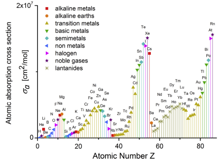
The EUV photoresists can be simply divided into organic photoresist, inorganic photoresist, and hybrid organic-inorganic photoresist according to its composition. Organic photoresists are mainly composed of carbon, hydrogen, and oxygen such as polymer and molecular glass, and they usually exhibit poor etch resistance with respect to a silicon substrate. With the improvement of photoresist resolution, the film of photoresist becomes thinner and thinner (~35 nm) to avoid high aspect ratio, while this trend makes it difficult for organic photoresists to tolerate etching conditions at this thickness [7]. In addition, pure inorganic photoresists such as metal halides[8], POSS[9], HafSOx[10-12] have been developed. But the sensitivity of these photoresists is too low for commercial applications. Moreover, solution stability and variable film moisture content will affect reproducibility and performance for HSQ and HafSOx. Unlike organic and inorganic photoresists, hybrid organic-inorganic photoresists exhibit more varied structures and complex properties. They contain both organic and inorganic components and combine both merits of organic and inorganic materials. On the one hand, inorganic elements usually have higher photoelectron absorption cross-sections than organics as shown in Figure 1 [13]. Elements with larger atomic absorption cross-section can improve the resist absorbance, which is favorable for the photoreaction. Meanwhile, the incorporation of inorganic units also improves the etch resistance. On the other hand, the organic parts of the photoresist can be easily adjusted to improve the performance such as solubility and sensitivity of the photoresist. Therefore, hybrid organic-inorganic photoresists as one of the most promising photoresists have attracted a lot of research in recent years. Ober et al. reviewed EUV photoresists for sub-7 nm patterning including some representative work in metal oxide nanoparticle photoresist [5]. Wei Liu and co-workers reviewed recent progress about inorganic photoresist materials, including their performance and working mechanism [7]. Robinson and Lawson give a detailed summary of materials and processes for next-generation lithography [14]. This review mainly focuses on the development of hybrid organic-inorganic photoresist over the past decade. In the following section, the hybrid photoresist materials are divided into metal nanoparticle/metal oxo-cluster photoresist, organometallic complex photoresist, and hybrid polymeric photoresist according to their molecular structure. Their photolithography properties and working mechanism are discussed here.


Figure 1.   Atomic absorption cross-sections σa for elements with atomic numbers from Z = 1 to 86. Reproduced from Reference [13].
2. Metal Nanoparticle and Metal Oxo-cluster Photoresist
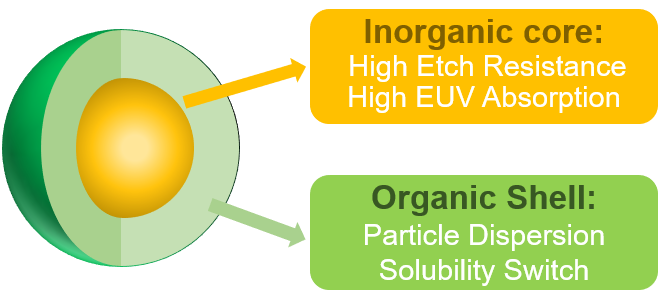
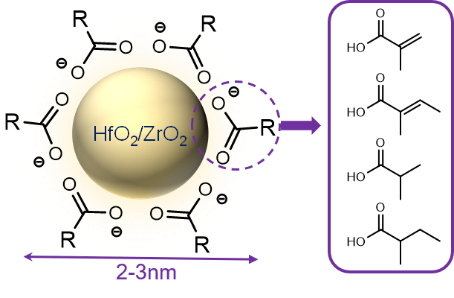
Metal nanoparticle and metal oxo-cluster photoresists are composed of inorganic metal core and organic ligands in the periphery as shown in Figure 2. The inorganic core provides the photoresist with high etching resistance and high EUV absorption, while the organic ligand is conducive to the dispersion of nanoparticles and the solubility change after exposure. According to the different metal elements contained in photoresists, they are simply divided into HfO2 and ZrO2 nanoparticle photoresists, Tin-oxo cluster photoresist and Zinc-based nanocluster photoresist.


Figure 2.   Schematic of metal nanoparticle or metal oxo-cluster.
2.1.   HfO2 and ZrO2 Nanoparticle Photoresists
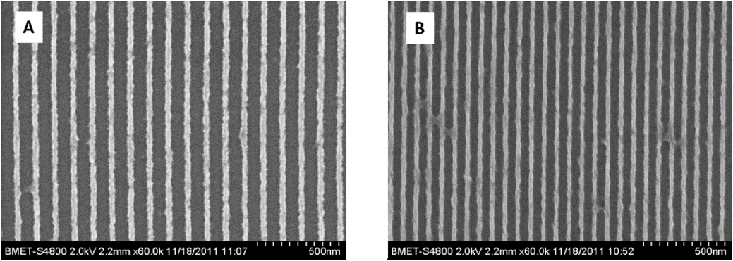
The Ober and Giannelis’s groups have developed many hybrid organic-inorganic photoresists based on ZrO2, HfO2 nanoparticle. They published the first article about the use of HfO2-based inorganic photoresist for DUV, EUV and E-beam lithography in 2010 [15]. The organic ligands of HfO2 nanoparticles were replaced by other carboxylic acids through a direct ligand exchange reaction. The particle diameter was between 1-3 nm and the size distribution was very narrow. Such a small particle was conducive to the improvement of lithography resolution. The positive and negative tone imaging were constructed by development in 0.26N TMAH for 30 sec (positive tone) or isopropyl alcohol for 2 min (negative tone). The required doses were reduced by the use of the radical photoinitiator DPAP. Compared with poly-hydroxy styrene (PHOST) films, the inorganic nanoparticle films are 2–3 times more resistant under the same conditions. The ZrO2, HfO2 nanoparticle photoresist for EUV lithography was studied in further research [16, 17]. The HfMAA and ZrMAA (MAA: methacrylic acid) nanoparticles could be used to form versatile dual-tone photoresists working with either radical photoinitiators or PAG additives. The ZrMAA films were patterned at a negative tone with 26 nm lines using a dose of 4.2 mJ/cm2 (Figure 3). The etch rate of the hafnium film is 0.17 nm/sec which is 25 times slower than the etch rate of the PHOST film using SF6/O2.


Figure 3.   
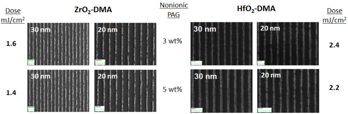
Negative tone patterns of the ZrMAA photoresist after EUV exposure: A) 32 nm lines at 5.6 mJ/cm2 and B) 26 nm lines at 4.2 mJ/cm2. Reproduced from Reference 17.
The hybrid photoresists based on ZrO2, HfO2 with different organic ligands were developed through a ligand exchange reaction. They prepared a HfO2-TDHT nanoparticle photoresist [18]. The nanoparticles were surface-functionalized with (S)-(+)-Tetrahydrofurfuryl-O-O’-diacetyl-(2R,3R)- hydrogentartrate (TDHT) via ligand exchange. The HfO2–TDHT showed good solubility in PGMEA and the film of HfO2–TDHT showed good uniformity. Dense 100 nm lines were achieved with this hybrid photoresist by e-beam lithography. ZrO2, HfO2 nanoparticle with trans-dimethylacrylic acid (DMA) and o-toluic acid ligands (TA) was also developed [19, 20].HfO2-DMA and ZrO2-DMA had high EUV sensitivity (1.6-2.4 mJ/cm2), and could produce high resolution line-space patterns (20 nm) with a compromise in pattern roughness (Figure 4). And nanoparticles with o-toluic acid ligand have lower sensitivity compared to the dimethylacrylate resists due to the strong binding affinity with the metal oxide core [21, 22].


Figure 4.   20 nm and 30 nm line-space patterns on ZrO2-DMA and HfO2-DMA resists films after EUV exposure. Reproduced from Reference [20].
Besides affecting the sensitivity of photoresist, surface ligands also affected the solubility of nanoparticles. Giannelis group had researched the solubility behavior of hybrid nanoparticles composed of a metal oxide core (ZrO2 or HfO2) and decorated with different carboxylic acids in different concentrations of photoacid generator as EUV photoresists. The structure of hybrid nanoparticles with different ligands is shown in Figure 5. The nanoparticles decorated with unsaturated surface ligands (MAA, DMA) showed more apparent solubility changes after being exposed to DUV than those with saturated ones, and the solubility change was more apparent in the film with a higher amount of photoacid generator [23].


Figure 5.   
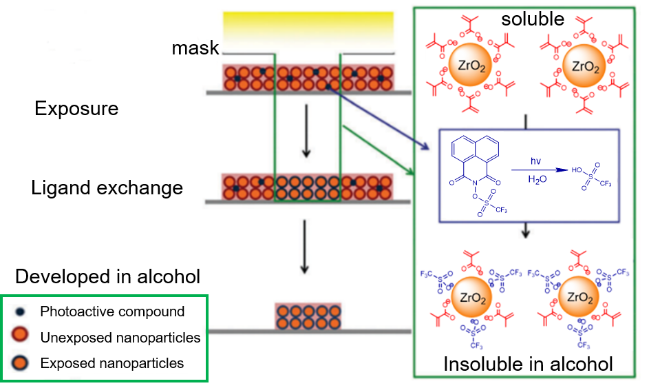
The structure of hybrid nanoparticles decorated with different carboxylic acids.
The patterning mechanism of these hybrid nanoparticles photoresists is complicated. The Ober and Giannelis’s group proposed the mechanism about the negative tone resists based on ligand exchange [24-26]. The photoactive compounds such as PAG or photo-radical generator released ligands that displaced surface ligands with a lower binding affinity (MAA) to nanoparticle cores and finally the ligand displacement resulted in the solubility difference between exposed and unexposed regions as shown in Figure 6 [27].


Figure 6.   
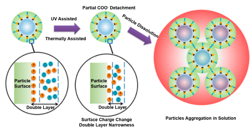
Schematic of the proposed mechanism for negative-tone pattern formation based on ligand exchange. Reproduced from Reference [27].
In the hybrid nanoparticles, the intrinsic chemical or morphological changes induced by UV exposure without the addition of photoactive compounds were also studied [28]. The particle sizes in solution showed a dramatic increase from the initial 3−4 nm to submicron size after exposure which was measured by dynamic light scattering. And XPS results showed that the carboxylic group on the surface of clusters decreased with increasing UV irradiation. A proposed mechanism was described in Figure 7. The detachment of small amounts of carboxylic groups changed the surface charge distribution of the nanoparticles, leading to suppression of electrostatic double layer width, and thus aggregation of the nanoparticles. Based on previous studies of mechanisms (ligand exchange, inorganic core condensation), Ober’s group further studied ZrO2 nanoparticle photoresist containing new materials such as photo-base generator (PBG) and high solubility PAG [29, 30]. The results confirmed that EUV lithography performance could be improved by adding appropriate PBG or high solubility PAG. It suggested that sol-gel condensation reaction could be catalyzed by base compounds and the acid released from PAG could displace surface ligands of nanoparticles.


Figure 7.   Proposed Mechanism for the hybrid HfO2 particle size increase after UV irradiation. Reproduced from Reference [28].
Chabal’s group reported a mechanistic investigation of the solubility switching reactions about Hf-MAA nanoparticle photoresist based on a combination of in situ IR spectroscopy, XPS, and DFT calculations. They found PAB treatment which was commonly used to remove residual solvent from resists could lead to condensation reactions, which in turn affected solubility and patterning. The main solubility switching mechanism was a crosslinking reaction initiated by decarboxylation of the methacrylate ligands under electron irradiation as shown in Figure 8. Although this crosslinking mechanism was different from the mechanism proposed by Ober and Gianelles, the mechanism of free radical induced polymerization was consistent with the previous observations [31]. Yamashita et al investigated the reaction mechanism of ZrOx–MAA resist under extreme ultraviolet (EUV) exposure by using hard X-ray photoelectron spectroscopy, near-edge X-ray absorption fine structure spectroscopy, and X-ray diffraction. They found EUV exposure decomposed the carbonyl species (MAA) and formed ZrO2 species [32].


Figure 8.   Proposed mechanism of the crosslinking reaction induced by electron beam irradiation. Reproduced from Reference [31].
2.2.   Tin-oxo Cluster Photoresists
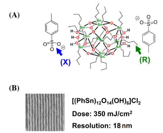
The first tin-oxo nanocluster photoresist used in EUV lithography was reported by Brainard’s group. They prepared several tin-oxo nanoclusters based on [(RSn)12O14(OH)6] X2 (R, organic ligands; X, carboxylic counter-anions) (Figure 9(A)). Compared with organic photoresist, tin-oxo nanoclusters can readily absorb EUV photons because their optical densities are 10.5 times greater than carbon (Figure 1). They proposed that more efficient utilization of the EUV photons gave better sensitivity and lower shot noise resulting in improved lithography performance. And tin-oxo nanoclusters were smaller and more uniform than hybrid ZrO2 /HfO2 nanoparticles so they should be capable of high resolution and low LER. To optimize the EUV lithographic performance and explore the photolysis mechanism of tin-oxo cluster resists, a series of tin-oxo clusters which varied bond energies of both the counter-ions (X) and the organic ligands (R) were synthesized and tested for EUV lithographic performance. No correlation was observed between the sensitivity of EUV imaging and the strength of the carbon–carbonyl bonds, but sensitivity was inversely proportional to the mass of the ligand. And resist sensitivity was also found to correlate directly with the organic ligand (R) bond energy. Therefore, it was speculated that the counter-ions only acted as non-reactive spacers inhibiting the clusters from combining and the photoreaction occurred with the tin-oxide cation. The homolysis of the tin–carbon bond produced tin-centered radicals and initiated cross-linking reactions, which caused agglomeration of the clusters, and finally resulted in the observed negative-tone imaging properties. The highest-resolution result for a tin-oxo cluster containing the phenyl organic ligands was 18-nm dense lines at 350 mJ/cm2 (Figure 9(B)). Although the sensitivity of tin-oxo clusters was poor, it was suggested that high-resolution resist materials as competitive as conventional organic polymers could be obtained by using highly sensitive ligands or alternate material sets [33, 34].


Figure 9.   
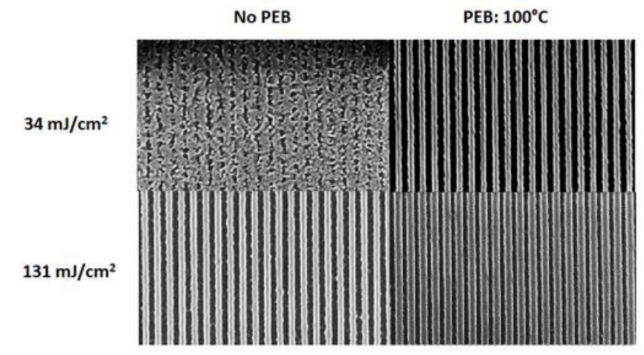
(A) The structure of tin-oxo nanoclusters. (B) Highest-resolution results for tin-oxo cluster containing the phenyl ligands. Reproduced from reference [33].
Further optimization of the processing conditions of tin-oxo cluster photoresist was studied by Brouwer et al [35]. PEB (post-exposure bake) was a step usually used in chemically amplified photoresists (CARs) to promote acid diffusion after exposure but not necessary for non-CARs. However, the result showed PEB had a significant effect on the sensitivity of the tin-oxo cluster photoresist (Figure 10). The pattern was not clear at doses of 34 mJ/cm2 without PEB, but the pattern was clearly visible if the sample was baked at 100˚ C (30 s) before development. At high exposure doses (131 mJ/cm2), the lines got wider after PEB, showing the effects of overexposure. A possible explanation was that photoreaction products were formed during EUV exposure, which could react further during the PEB step. Development was another important step that affected lithography performance. The authors found the bridging effect can be effectively reduced by increasing the rinsing time in the process of development. Brouwer’s group also reported the dual-done property of the tin-oxo cluster photoresist in EUV lithography and e-beam lithography [36]. The tin-oxo cluster [(RSn)12O14(OH)6] (OH)2 could not only be used as a positive photoresist at low exposure dose but also achieve negative patterns at high exposure dose. At high exposure dose, a large amount of carbon loss was detected by XPS, which was due to the breaking of the tin-carbon bond caused by radiation. The exposed area was insoluble after exposure, so it was used as a negative photoresist. At a low exposure dose, the unexposed area was insoluble after high temperature PEB treatment, while the exposure area could still be dissolved. This was because radiation changed the heat sensitivity of the material in the exposed area, and this small change ultimately affected the dissolution behavior and finally achieved positive patterns. The more exact mechanism of positive photoresist will be studied in the future.


Figure 10.   
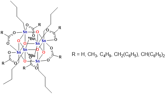
The effect of PEB on [(RSn)12O14(OH)6] (OH)2 resist at two different doses (34 mJ/cm2 and 131 mJ/cm2) for 50 nm half-pitch lines. Reproduced from Reference [35].
Johnson’s group prepared a series of organotin compounds [n-BuSn(O)O2CR]6 (Figure 11) and the crystal structure of these tin clusters was examined by single crystal X-ray diffraction (XRD) [37]. The crystal structures of these clusters helped to understand how the size and structure of ligands affected the packing structure and density. The packing structure and density may be affected the efficiency of crosslinking of the inorganic metal cores and the decomposition of organic ligands. Meanwhile, Johnson and Hutchison’s team compared three organotin carboxylate species [(nBuSn)12O14 (OH)6]2+(CH3COO)2, [nBuSn(O)O2CCH3]6, n-Bu2Sn(O2CCH3)2 with the same organic ligand but different metal cores to understand how the structure affected chemical transformations that occurred during patterning [38]. The results showed that both the metal-oxo core and the ligand of each organotin compound affected the reaction efficiency during electron beam patterning. The metal-oxo core affected the sensitivity to the electron beam. Tin-oxo cluster, [(nBuSn)12O14(OH)6]2+(CH3COO)2 had the highest sensitivity at a dose of 12 μC/cm2 because it had more Sn-O-Sn bonds and the carboxyl ligand with weak coordination. After exposure, the butyl ligands of organotin compound decomposed, while about 60% remained in the film which was examined by electron-stimulated desorption. The organotin compounds with the residual ligands may be crosslinked to form a metal-oxo polymer. The polymer patterns can be converted into inorganic oxides by heating the films at 300 °C or oxygen plasma treatment [39].


Figure 11.   The structure of organotin clusters with different carboxylic ligands.
A charge-neutral, butyl-tin Keggin (β-NaSn13) nanocluster synthesized by Herman et al, was used as a EUV photoresist to better understand the photoreactions caused by radiation and the influence of ambient conditions on the sensitivity of photoresist [40, 41]. Compared with UHV, the exposure dose required for the β-NaSn13 nanocluster photoresist in an oxygen ambient was significantly reduced. They believed that the change in sensitivity was attributed to the reactive oxygen species that were generated by molecular oxygen induced by electron radiation and the hydrogen extraction reaction of butyl ligands.
2.3.   Zinc-based Nanocluster Photoresists
In recent years, nanocluster photoresists based on Zn have been investigated and have shown promising results [42-48]. A Zn oxo-cluster photoresist was synthesized by Soppera’s group in 2016 [42, 43]. Zinc methacrylate (ZnMAA) was used as the precursor and Zn oxo-cluster was formed via hydrolysis–condensation reaction. After DUV exposures, the crosslinking-aggregation of Zn oxo-cluster occurred and the M-O-M network was formed in exposed regions. The organic part in the film could be completely removed after annealing, leading to the formation of ZnO with semiconducting properties.
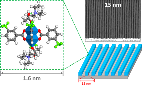
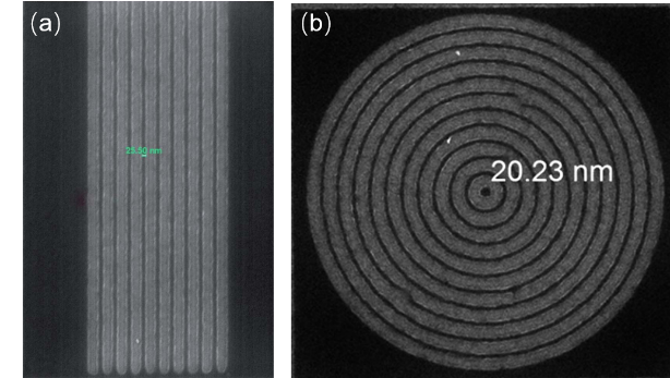
By replacing the bridging ligand of MOF-2 with monovalent ligands, Ober et al prepared two zinc-based clusters used as photoresist material for extreme ultraviolet lithography [45]. The first one was the phenyl-modified Zn2(CO2)4 called Zn-BA, the other was 3-methyl-phenyl-modified Zn2(CO2)4 called Zn-mTA. Compared with Zn-BA, Zn-mTA cluster showed extremely high solubility in organic solvents and better film uniformity due to the twisted structure and configurational isomers. Therefore, Zn-mTA had better photolithography performance, and 15 nm lines could be achieved under a dose of 47 mJ/cm2 in EUV lithography (Figure 12). Many advantages of Zn-mTA cluster such as small size, narrow size distribution and homogeneous film gave it a higher resolution than the HfO2 and ZrO2 nanoparticle. The proposed mechanism of the negative-tone pattern was the acid generated by PAG reacted with the Zn-mTA cluster via ligand exchange reaction, which changed the charge distribution on the surface of the nanoclusters and reduced its solubility in non-polar solvents.


Figure 12.   
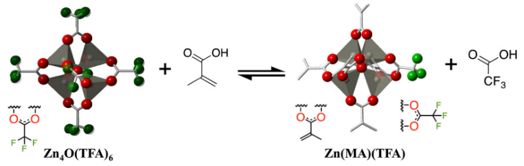
The structure of Zn-mTA cluster and 15 nm line-and-space dense patterns of the Zn-mTA cluster. Reproduced from Reference [45].
Castellanos et al. investigated a new hybrid photoresist based on zinc metal oxo-clusters [48]. The cluster Zn(MA)(TFA) was synthesized by ligand-exchange reactions as shown in Figure 13. The Zn metallic oxo core and trifluoroacetate (TFA) ligands enhanced the EUV absorbance of the film because both zinc and fluorine had a high EUV photon absorption cross section. The introduction of methacrylate ligands (MA) with a terminal double bond could achieve better solubility conversion due to the polymerization and crosslinking of double bonds. The stability of the bulk material and the thin films were studied by UV–vis absorption and FTIR spectroscopy. The results showed Zn (MA)(TFA) cluster could be partially hydrolyzed by the moisture in the air and natural light in the environment could cause the aggregation of MA ligands. Nonetheless, the film of clusters was stable in air or vacuum for several hours. The pattern of 30 nm half-pitch could be achieved under a dose of 37 mJ/cm2 in EUV lithography but different batches of nanoclusters synthesized by the same process showed significant variations due to the small difference of organic shells in different batches of nanoclusters. This research indicated that the inorganic nanoclusters are very sensitive to structural changes which should be controlled to obtain reproducible lithographic results.


Figure 13.   Scheme of the synthesis of Zn (MA)(TFA) nanocluster based on ligand-exchange reactions. Reproduced from Reference [48].
3.   Organometallic Complex Photoresist
Organometallic complex photoresists usually contain at least one metal atom with high EUV optical density and photosensitive organic ligand coordinated with the metal atom. Brainard’s group developed a class of organometallic complexes based on the metal bismuth [49], antimony [50], tin [51], tellurium, platinum, palladium [52], cobalt, iron and chromium [53-55] for EUV lithography.
Bismuth complexes: The bismuth complexes were designed by two approaches as shown in Figure 14. Approach 1 was based on the acid instability of bismuth-phenyl bond. The acid produced by the PAG during exposure caused the decomposition of bismuth-phenyl bond and thus changed the solubility of the exposed region. It was not suitable for EUV lithography because of the poor EUV sensitivity and a high wt% of PAG must be used due to the noncatalytic nature. Several bismuth oligomers were designed based on Approach 2 (intermolecular cross-linking). The oligomers where X = Cl or OOC-R showed poor resolution of 100 nm at the dose of 30 mJ/cm2 (X = OOC-R) and modest resolution of 21 nm at the dose of 120 mJ/cm2 (X = Cl) [49, 56].


Figure 14.   Two approaches taken to develop new bismuth complex resists (X = Cl or OOC-R). Reproduced from Reference [49].
Antimony complexes: A set of organometallic carboxylate compounds [Rn Sb(O2CR’)2] were also developed by Brainard's group. They studied organometallic carboxylate compounds of the general form [Rn M(O2CR’)2] with different M, R, and R’. Compared with the PhnM(acrylate)2 where M = bismuth, tin, or tellurium, the PhnSb(acrylate)2 was the most sensitive. By optimizing the structure of R and R’, they found the carboxylic ligand containing polymerizable olefin double bonds showed better sensitivity and 35-nm dense lines could be achieved under a dose of 5.6 mJ/cm2(Figure 15) [50]. A possible mechanism for the high sensitivity of antimony complexes containing polymerizable olefin double bonds was the polymerization of double bonds in antimony complexes. Also, antimony carboxylate molecules like tri(phenyl)antimony diacetate which didn’t contain a polymerizable group also showed good sensitivity (Emax = 21 mJ/cm2). Therefore, the photolysis mechanism of antimony carboxylate without the polymerizable group was studied by analyzing volatile products during exposure [57, 58]. Outgassing experiments by mass spectrometry confirmed that the major volatile products were CO2, benzene, and phenol, there was a strong correlation between decarboxylation activation energy and the rate of outgassing. And they proposed the reaction pathways to form benzene and phenol based on isotopic labeling studies of antimony complexes[59, 60].


Figure 15.   The structure and pattern of the Ph3Sb(acrylate)2 resist with high sensitivity. Reproduced from Reference [50].
Platinum and palladium complexes: Brainard et al studied platinum and palladium mononuclear complexes with different ligands including cis, cis-1,5-cyclooctadiene (COD), azide (N3), carbonate (CO32- ), and oxalate (C2O42- ) [52]. The platinum and palladium complexes containing COD and N3 had poor EUV sensitivity. The metal carbonates exhibited negative-tone behavior while metal oxalates endowed positive-tone patterns with better sensitivity (Figure 16). And the result showed palladium complex resists were more sensitive than platinum complex resists. 30-nm dense lines could be patterned by using palladium complex (dppm)Pd(C2O4) (dppm =1,1-bis(diphenylphosphino)methane) at the dose of 50 mJ/cm2. According to mass spectrometry and NMR data, the result suggested the loss of CO2 and the formation of a L4Pd complex during EUV exposure.


Figure 16.   The structure of L2M(CO3) and L2M(C2O4) complexes.
Tin complexes: Due to the etch resistance and high-EUV optical density, tin complexes had great potential to create photoresist with better resolution, sensitivity, and LER. A series of mononuclear tin complexes, R2Sn(O2CR’)2 were synthesized for EUV lithography. By studying tin complexes with different ligands (R= phenyl, butyl, benzyl), it was found that the sensitivity was linearly related to the molecular weight of the carboxyl group and the free radical stability of the hydrocarbon group bound to tin. Although the sensitivity of many of these tin complexes was poor, they achieved 1.4 nm LER at 22-nm half-pitch patterning and good LER of 1.1 nm at 35-nm half-pitch at the dose of 600 mJ/cm2 (Figure 17). The sensitivity can be significantly improved (about 5~30 mJ/cm2) by introducing ligands containing olefins [51]. Herman et al. investigated the patterning mechanism of butyl-tin oxide hydroxide (BuSnOOH) under radiation. The temperature programmed desorption (TPD) results indicated BuSnOOH had good thermal stability and the cleavage of the butyl-tin bond in BuSnOOH occurred at ~653 K. According to the XPS results, the main reasons for the change of solubility after exposure were the loss of butyl group and the increase of tin-oxygen network [61].


Figure 17.   (a) The structure of tin complex, (C6H5CH2)2Sn(O2C(C(CH3)3))2 and (b) its high resolution patterning with extremely low LER. Reproduced from Reference [51].
Cobalt, iron, and chromium complexes: Transition metal-oxalates are sensitive to UV–Vis light, and the oxalate ligands of these complexes would be converted to CO2 and two electrons under UV –Vis light [62, 63]. Brainard et al developed a set of inorganic oxalate complexes, M(oxalate)m(bpy)n, where m+n= 3, bpy= 2,2’-bipyridine and M= Co, Fe or Cr, as negative-tone extreme ultraviolet (EUV) resists [53, 54]. According to the results of EUV lithography, the sensitivity of these oxalate complexes increased with the number of oxalate ligands and cobalt complexes exhibited better sensitivity than analogous chromium and iron complexes (Figure 18). The most successful complex in lithographic studies is [PPh3(CH2Ph)][Co(oxalate)2(bpy)], which achieved 20 nm h/p lines at the dose of 30 mJ/cm2. The results of infrared, paramagnetic nuclear magnetic resonance, and cyclic voltammetric studies showed EUV exposure caused oxalate ligands to decompose into CO2 and resulted in the decomposition products of Co(II)(2,2’-bipyridine)(oxalate) and [PPh3(CH2Ph)]2(oxalate).


Figure 18.   35-nm h/p lines for [PPh3(CH2Ph)][M(oxalate)2(bpy)],where M is Co, Fe or Cr. Reproduced from Reference [53].
4.   Hybrid Polymeric Photoresists
In DUV lithography, almost all resists were based on polymeric resins. Polymers have many fabulous properties, such as forming a uniform amorphous film easily by spin coating and high glass transition temperature for processing, which make them suitable as photoresist. Around the year 2000, some hybrid polymer photoresists containing silicon were developed to increase the transparency of the polymer because of the low EUV absorption of silicon [64-66]. With the continuous improvement of lithography resolution, this idea is no longer applicable, because the photoresist film becomes thinner and thinner which makes the transparency unnecessary. Meanwhile, the etching resistance of the photoresist becomes more important. However, polymeric photoresists which are mainly composed of carbon, hydrogen and oxygen have poor etching resistance. Therefore, many hybrid polymeric photoresists have been developed to improve the performance (sensitivity, etch resistance) of polymeric photoresists by incorporating inorganic components.
Gonsalves et al. developed a series of sulfonium based negative tone polymeric photoresists by varying polymer microstructures for e-beam and EUV lithography [67-71]. They found that the polymer incorporated with ferrocene had better thermal stability and sensitivity than the (4-(methacryloyloxy) phenyl)dimethylsulfonium triflate (MAPDST) homopolymer. The MAPDST-FMMA copolymer could pattern 25 nm line features under EUV exposure (Figure 19(a)) [72]. In addition to incorporating ferrocene into the polymer backbone, Gonsalves’s team had also developed other hybrid polymeric resists containing polyoxometalate [73], HfO2 nanoparticle [74] and hexafluoroantimonate [75]. The structure of these hybrid polymeric photoresists were shown in Figure 20. The hybrid polymeric resist containing polyoxometalate showed better performance because polyoxometalates could capture EUV photons more efficiently, improve glass transition temperatures, enhance decomposition temperature and etch resistance [73]. 20 nm circular images with 70 nm space was patterned under EUV exposure as shown in Figure 19(b). Moreover, the sensitivity of the polymer photoresist containing inorganic counter ion hexafluoroantimonate was significantly improved due to the larger atomic absorption cross-section of Sb. The sensitivity of the hybrid photoresists containing 1.5% and 2.15% hexafluoroantimonate were 58.1 mJ/cm2 and 24.5 mJ/cm2, respectively. High resolution 20 nm lines and other nano scale patterns such as waves, dots, rings could be realized with these hybrid photoresists [75].


Figure 19.   EUV exposure results for MAPDST resists containing (a) FMMA or (b)polyoxometalate. Reproduced from Reference [72,73].


Figure 20.   The structure of hybrid polymeric photoresists containing ferrocene, polyoxometalate, HfO2 nanoparticle, hexafluoroantimonate.
Polyhedral oligomeric silsesquioxane (POSS) is an inorganic electron beam photoresist with excellent etching resistance. A series of POSS-containing polymeric photoresists were synthesized by the ways of copolymerization, grafting, or blending [76-80]. The introduction of POSS units into the polymers could enhance the etching resistance and change other properties such as sensitivity [79], thermal and mechanical stability [78]. Cui et al. developed an organometallic metal carbonyl polymer, PFpP, for high resolution positive and negative electron beam lithography. The PFpP resist exhibited about 20 times stronger resistance to oxygen dry etching than organic photoresist, e.g. PMMA and ZEP-520A. Another significant feature was its high resolution, which allowed for a 17 nm line pattern exposed at 15 nC/cm [81].
5.   Conclusion and Outlook
This review summarizes the recent development of organic-inorganic hybrid photoresists in EUV lithography. The research of EUV photoresist is facing numerous challenges that hinder the improvement of photoresist performance such as electron and acid blur, pattern collapse at high aspect ratios, and photon shot noise. Meanwhile, photoresist needs to meet the performance requirements of the resolution, sensitivity, and LER for future semiconductor device technology nodes. Organic photoresists used in EUV lithography are limited due to its low etching resistance and inherent tradeoff relationships among resolution, sensitivity, and LER in CARs. Compared with organic photoresist, organic-inorganic hybrid photoresist shows great potential for EUV photoresist due to its more variable and adjustable structure and properties of materials by changing the metal center and organic ligands. The hybrid photoresists discussed in this review such as metal nanoparticles, metal oxo-clusters, and organometallic complexes all showed excellent lithographic performance. Some of the properties of hybrid photoresists were summarized in Table 1 for clarity. Recently, 8 nm half-pitch lines have been successfully printed by using 11 nm thick MOx resist. From the current developments’ point of view, hybrid photoresists show many attractive characteristics but need further development. There are many questions such as the chemical mechanisms, the structures of the insoluble materials, and the role of secondary electrons et al, need to be further studied. With the improvement of the resolution of photoresists, Moore's Law may be nearing its end, and the era of molecular and atomic patterning is coming.
Table 1.   Summary of organic-inorganic hybrid EUV resists a
ResistSensitivity (mJ/cm2)Resolution(nm)LER
(nm)
ToneTd
(OC)
Ref
HfMAA731-negative-15, 22
ZrMAA4.2263.8negative-16, 17
Tin-oxo nanocluster35018-negative-34
Zn-mTA cluster4715-negative>11045
Zn (MA)(TFA) nanocluster3730-negative>12548
Ph3Sb(acrylate)25.635-negative-50
(dppm)Pd(C2O4)5030-positive-52
(C6H5CH2)2Sn(O2C(C(CH3)3))2600221.4negative-51
[PPh3(CH2Ph)][Co(oxalate)2(bpy)]35225.4negative-53
MAPDST–FMMA copolymer-253.0negative22672
POM/polymer hybrids8.520-negative25073
MAPDSA–MAPDST copolymer24.5201.53-5.18negative>24075
a All the data are from the references, and properties not provided in references are replaced by dashes.
Acknowledgments
Financial support from the National Natural Science Foundation of China (22090012, U20A20144, 21873106, 22073108 and 21903085) and the Ministry of Science and Technology of China Major Project (2018ZX02102005; 2011ZX02701) is gratefully acknowledged. J.C. and Y.Z. acknowledges the support of the Youth Innovation Promotion Association, CAS.
Acknowledgments
[1] R. R. Schaller, “Moore’s law: past, present and future,”IEEE Spectrum. 34 (6), 52–59 (1997).
[2] S. E. Thompson, S. J. M. T. Parthasarathy, “Moore's law: The future of Si microelectronics,” Materials Today. 9, 20-25 (2006).
[3] C. Mack, Fundamental Principles of Optical Lithography: The Science of Microfabrication, John Wiley & Sons, Ltd, (2007).
[4] S. J. J. o. V. S. Okazakiet al., “Resolution limits of optical lithography,” J. Vac. Sci. Technol B.9 (6), 2829-2833 (1991).
[5] L. Liet al., “Extreme ultraviolet resist materials for sub-7 nm patterning,” Chem Soc Rev.46 (16), 4855-4866 (2017).
[6] A. Reiseret al., “Novolak-diazoquinone resists: the imaging systems of the computer chip,” Angew. Chem. Int . Ed.35 (21), 2428-2440 (1996).
[7] C. Luo et al., “Review of recent advances in inorganic photoresists,” Rsc Adv.10 (14), 8385-8395 (2020).
[8] A. Murayet al., “Radiolysis and resolution limits of inorganic halide resists,” J. Vac. Sci. Technol B.3 (1), 367-372 (1985).
[9] A. E. Grigorescu, C. W. Hagen, “Resists for sub-20-nm electron beam lithography with a focus on HSQ: state of the art, ” Nanotechnology.20 (29), 292001 (2009).
[10] R. P. Oleksaket al., “Chemical and structural investigation of high-resolution patterning with HafSOx, ” Acs Appl Mater Inter.6 (4), 2917-2921 (2014).
[11] J. Stowers, D. A. J. M. E. Keszler, “High resolution, high sensitivity inorganic resists,” Microelectronic Engineering. 86(4-6), 730–733(2009).
[12] J. K. Stowerset al., Extreme Ultraviolet, B. M. LaFontaine, P. P. Naulleau, Eds. Spie-Int Soc Optical Engineering, Bellingham, (2011).
[13] Fallicaet al., “Absorption coefficient of metal-containing photoresists in the extreme ultraviolet,” J. Micro/Nanolith. MEMS MOEMS. 17(2), 023505 (2018).
[14] A. Robinson, R. Lawson, Materials and Processes for Next Generation Lithography, Elsevier, Amsterdam, Netherlands (2016).
[15] M. Trikeriotiset al., “Development of an inorganic photoresist for DUV, EUV, and electron beam imaging,” Proc. of SPIE.7639 , 76390E (2010).
[16] M. Trikeriotiset al., “A new inorganic EUV resist with high-etch resistance,” Proc. of SPIE. 8322 , 83220U (2012).
[17] M. Trikeriotiset al., “Nanoparticle photoresists from HfO2 and ZrO2 for EUV patterning,” J Photopolym Sci Tec.25 (5), 583-586 (2012).
[18] W. J. Baeet al., “High refractive index and high transparency HfO2 nanocomposites for next generation lithography,” J Mater Chem.20 (25), 5186-5189 (2010).
[19] J. Jianget al., “Metal oxide nanoparticle photoresists for EUV patterning,” J Photopolym Sci Tec.27 (5), 663-666 (2014).
[20] S. Chakrabartyet al., “Increasing sensitivity of oxide nanoparticle photoresists,” Proc. of SPIE. 9048, 90481C (2014).
[21] J. Jianget al., “Oxide nanoparticle EUV (ONE) photoresists: current understanding of the unusual patterning mechanism,” J Photopolym Sci Tec.28 (4), 515-518 (2015).
[22] B. Cardineauet al., “Tightly-bound ligands for hafnium nanoparticle EUV resists,” Proc. of SPIE. 8322 , 83220V (2012).
[23] L. Liet al., “Solubility studies of inorganic-organic hybrid nanoparticle photoresists with different surface functional groups,” Nanoscale.8 (3), 1338-1343 (2016).
[24] M. Kryasket al., “Nanoparticle photoresists: ligand exchange as a new and sensitive EUV patterning mechanism,” J Photopolym Sci Tec.26 (5), 659-664 (2013).
[25] S. Chakrabartyet al., “Oxide nanoparticle EUV resists: toward understanding the mechanism of positive and negative tone patterning,” Proc. of SPIE.8679 , 867906 (2013).
[26] M. Yu, E. P. Giannelis, C. K. Ober,“Positive tone oxide nanoparticle EUV (ONE) photoresists,”Proc. of SPIE. 9779, 977905 (2016).
[27] C. Ober, E. J. S. N. Giannelis, “New oxide nanoparticle extreme-UV photoresists achieve high sensitivity,” SPIE Newsroom. (2014).
[28] L. Liet al., “Studying the mechanism of hybrid nanoparticle photoresists: effect of particle size on photopatterning,” Chem Mater.27 (14), 5027-5031 (2015).
[29] K. Kasaharaet al., “Recent progress in EUV metal oxide photoresists,” J Photopolym Sci Tec.30 (1), 93-97 (2017).
[30] K. Kasaharaet al., “Recent progress in nanoparticle photoresist development for EUV lithography,” Proc. of SPIE. 9776 , 977604 (2016).
[31] E. C. Mattsonet al., “Chemical modification mechanisms in hybrid hafnium oxo-methacrylate nanocluster photoresists for extreme ultraviolet patterning,” Chem Mater.30 (17), 6192-6206 (2018).
[32] Y. Yamashitaet al., “Reaction mechanism of ZrOx metal resists with extreme ultraviolet irradiation,” Jpn J Appl Phys.58 , (2019).
[33] B. Cardineauet al., “EUV resists based on tin-oxo clusters, ” Proc. of SPIE.9051 , 90511B (2014).
[34] B. Cardineauet al., “Photolithographic properties of tin-oxo clusters using extreme ultraviolet light (13.5nm),” Microelectronic Engineering.127 , 44-50 (2014).
[35] J. Haitjemaet al., “Extreme ultraviolet patterning of tin-oxo cages,” J. of Micro/Nanolithography, MEMS, and MOEMS.16 (3), 033510 (2017).
[36] Y. Zhanget al., “Dual-tone application of a tin-oxo cage photoresist under E-beam and EUV exposure,” J Photopolym Sci Tec.31 (2), 249-255 (2018).
[37] M. C. Sharps et al., “Implications of crystal structure on organotin carboxylate photoresists,” Crystal Research and Technology.52 (10), 1700081 (2017).
[38] M. C. Sharpset al., “Organotin carboxylate reagents for nanopatterning: chemical transformations during direct-write electron beam processes,” Chem Mater.31 (13), 4840-4850 (2019).
[39] C. Y. Namet al., “Direct fabrication of high aspect-ratio metal oxide nanopatterns via sequential infiltration synthesis in lithographically defined SU-8 templates,” J. Vac. Sci. Technol. B.33 (6), 241-256 (2015).
[40] J. T. Diuluset al., “Effect of ambient conditions on radiation-induced chemistries of a nanocluster organotin photoresist for next-generation EUV nanolithography,” Acs Applied Nano Materials.3 (3), 2266-2277 (2020).
[41] R. T. Frederick et al., “Effect of oxygen on thermal and radiation-induced chemistries in a model organotin photoresist,” Acs Appl Mater Inter.11 (4), 4514-4522 (2019).
[42] C. C. Yehet al., “Controllable formation of zinc oxide micro- and nanostructures via DUV direct patterning,” Adv Mater Interfaces.3 (19), 1600373 (2016).
[43] C. C. Yehet al., “Chemical and structural investigation of zinc-oxo cluster photoresists for DUV lithography,” J Mater Chem C.5 (10), 2611-2619 (2017).
[44] K. Sakaiet al., “Progress in metal organic cluster EUV photoresists,” J Vac Sci Technol B.36 (6), 06J504 (2018).
[45] H. Xuet al., “Metal-organic framework-inspired metal-containing clusters for high-resolution patterning,” Chem Mater.30 (12), 4124-4133 (2018).
[46] V. Kosma, D. De Simone, G. Vandenberghe,“Metal based materials for EUV lithography,” J Photopolym Sci Tec.32 (1), 179-183 (2019).
[47] K. Sakaiet al., “Metal organic cluster photoresists for EUV lithography,” J Photopolym Sci Tec.32 (5), 711-714 (2019).
[48] N. Thakur et al., “Stability studies on a sensitive EUV photoresist based on zinc metal oxoclusters,” J. of Micro/Nanolithography, MEMS, and MOEMS.18 (4), 043504 (2019).
[49] J. Passarelliet al., “EUV resists comprised of main group organometallic oligomeric materials,” Proc. of SPIE.9051 , 90512A (2014).
[50] J. Passarelliet al., “Organometallic carboxylate resists for extreme ultraviolet with high sensitivity,” J. Micro/Nanolith. MEMS MOEMS. 14 (4), 043503 (2015).
[51] R. Del Reet al., “Low-line edge roughness extreme ultraviolet photoresists of organotin carboxylates,” J. Micro/Nanolith. MEMS MOEMS. 14 (4), 043506 (2015).
[52] M. Sortlandet al., “Platinum and palladium oxalates: positive-tone extreme ultraviolet resists,” J. Micro/Nanolith. MEMS MOEMS.14 (4), 043511 (2015).
[53] M. Wilklow-Marnellet al., “First-row transitional-metal oxalate resists for EUV, ” J. Micro/Nanolith. MEMS MOEMS. 17 (4), 043507 (2018).
[54] S. Grzeskowiaket al., “Reactivity of metal oxalate EUV resists as a function of the central metal,” Proc. of SPIE.10146 , 1014605 (2017).
[55] B. Cardineau, Materials and Processes for Next Generation Lithography, A. Robinson, R. Lawson, Eds, Elsevier Ltd (2016).
[56] J. Passarelliet al., “Bismuth resists for EUV lithography, ” J Photopolym Sci Tec.27 (5), 655-661 (2014).
[57] Schuleret al., “EUV mechanistic studies of antimony resists, ” J Photopolym Sci Tec.30 (1), 121-131 (2017).
[58] E. M. Panninget al., “Antimony photoresists for EUV lithography: mechanistic studies,”Proc. SPIE. 10143, 1014307 (2017).
[59] M. Murphyet al., “Mechanisms of photodecomposition of metal-containing EUV photoresists: isotopic labelling studies, ” Proc. SPIE.10586 , 1058608 (2018).
[60] M. Murphyet al., “Isotopic labeling studies of EUV photoresists containing antimony,” J Photopolym Sci Tec.31 (2), 233-242 (2018).
[61] R. T. Fredericket al., “Thermal and radiation chemistry of butyltin oxo hydroxo: A model inorganic photoresist,” Microelectronic Engineering.205 , 26-31 (2019).
[62] A. L. Poznyak, V. I. Pavlovski, “Photochemical reactions of ligands in transition-metal complexes,” Angewandte Chemie-International Edition in English.27 (6), 789-796 (1988).
[63] E. L. Simmons, Wendland.Ww, “Solid-state photochemical reactions of transition-metal coordination compounds,” Coordin Chem Rev.7 (1), 11-27 (1971).
[64] Y. J. Kwarket al., “Novel silicon containing polymers as photoresist materials for extreme UV lithography, ” Proceedings of SPIE. 5039, 1204-1211 (2003).
[65] A. Yamaguchiet al., “Self-developing characteristics of Si containing polymers and their application to x-ray lithography,” J. Electrochem. Soc. 143(2), 657-665 (1996).
[66] J. Y. Daiet al., “Synthesis and evaluation of novel organoelement resists for EUV lithography, ”Proc. SPIE. 5039 , 1164-1172 (2003).
[67] V. S. V. Satyanarayanaet al., “Radiation-sensitive novel polymeric resist materials: iterative synthesis and their EUV fragmentation studies,” ACS Appl. Mater. Interfaces6 (6), 4223-4232 (2014).
[68] V. S. V. Satyanarayanaet al., “Organic-inorganic hybrid resists for EUVL,” Proc. SPIE. 9051 ,90511W (2014).
[69] V. Singhet al., “Optimization of processing parameters and metrology for novel NCA negative resists for NGL,”Proc. SPIE. 9048 ,90481Y (2014).
[70] V. Singhet al., “Towards novel non-chemically amplified (n-CARS) negative resists for electron beam lithography applications,” J. Mater. Chem. C. 2(12), 2118 (2014).
[71] S. Ghoshet al., “Patterning highly ordered arrays of complex nanofeatures through EUV directed polarity switching of non chemically amplified photoresist,” Scientific Reports. 6(1), 22664 (2016).
[72] V. S. V. Satyanarayanaet al., “A hybrid polymeric material bearing a ferrocene-based pendant organometallic functionality: synthesis and applications in nanopatterning using EUV lithography,” Rsc Adv.4 (104), 59817-59820 (2014).
[73] Vishwanathet al., “New polyoxometalates containing hybrid polymers and their potential for nano-patterning,” Chem. Eur. J.21 (5), 2250 – 2258 (2015).
[74] P. G. Reddyet al., “Design, development, EUVL applications and nano mechanical properties of a new HfO2 based hybrid non-chemically amplified resist,” Rsc Adv.6 (71), 67143-67149 (2016).
[75] P. G. Reddyet al., “Organic-inorganic hybrid photoresists containing hexafluoroantimonate: design, synthesis and high resolution EUV lithography studies,” Materials Chemistry Frontiers.1 , 2613-2619 (2017).
[76] E. Tegouet al., “Polyhedral oligomeric silsesquioxane (POSS) based resists: material design challenges and lithographic evaluation at 157 nm,” Chem. Mater.16 (13), 2567-2577 (2004).
[77] E. Tegouet al., “Polyhedral oligomeric silsesquioxane (POSS) acrylate copolymers for microfabrication: properties and formulation of resist materials,” Microelectronic Engineering.73–74 , 238–243 (2004).
[78] N. Yong, S. Zheng, K. J. P. Nie, “Morphology and thermal properties of inorganic–organic hybrids involving epoxy resin and polyhedral oligomeric silsesquioxanes,” Polymer.45 (16), 5557-5568 (2004).
[79] H. M. Lin, K. H. Hseih, F. C. J. M. E. Chang, “Characterization of negative-type photoresists containing polyhedral oligomeric silsesquioxane methacrylate,” Microelectronic Engineering. 85, 1624-1628 (2008).
[80] S. A. Woo, S. Y. Choi, J.-B. Kim, “Non-chemically amplified resists containing polyhedral oligomeric silsesquioxane for a bilayer resist system,” Polymer.98 , 336-343 (2016).
[81] J. Zhanget al., “Metal-carbonyl organometallic polymers, PFpP, as resists for high-resolution positive and negative electron beam lithography, ” Chem. Commun. 51 (99), 17592-17595, (2015).
Article and author information
Zhihao Wang
Xindi Yao
Huiwen An
Yake Wang
Jinping Chen
Shuangqing Wang
Xudong Guo
Tianjun Yu
Yi Zeng
Guoqiang Yang
Yi Li
Publication records
Published: March 28, 2021 (Versions1
References
Journal of Microelectronic Manufacturing