There are demands for high brightness, stable, long-life and broadband light sources in advanced applications of semiconductor metrology, sensor calibration, materials science and life science research. Laser-driven light sources are capable of delivering super-high brightness and stable radiation with long lifetimes. LDLS sources use high power diode lasers or fiber lasers to energize high-intensity Xe plasma which in turn produces broadband radiation from 170nm to 2400nm.
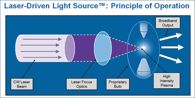
Due to its design principle, an LDLS plasma is not sustained by electric currents going through Xe bulb electrodes but by direct plasma absorption of the focused laser optical energy, Figure 1. As an analogy, the principle is somewhat similar to a laser metal welding where liquefied metal at the laser focal spot absorbs the laser energy and reaches its melting temperature.
This novel design of energy delivery method eliminates electrode material vaporization and sputtering during lamp operation, so the Xe bulb wall remains clean. The Xe plasma in an LDLS also has higher spatial and temporal stability due to the elimination of plasma and electrode interactions experienced in conventional short arc lamps. An LDLS plasma is energized at a higher power density due to the sharply focused laser beam, so the plasma core temperature is much higher than a DC short-arc Xe lamp plasma
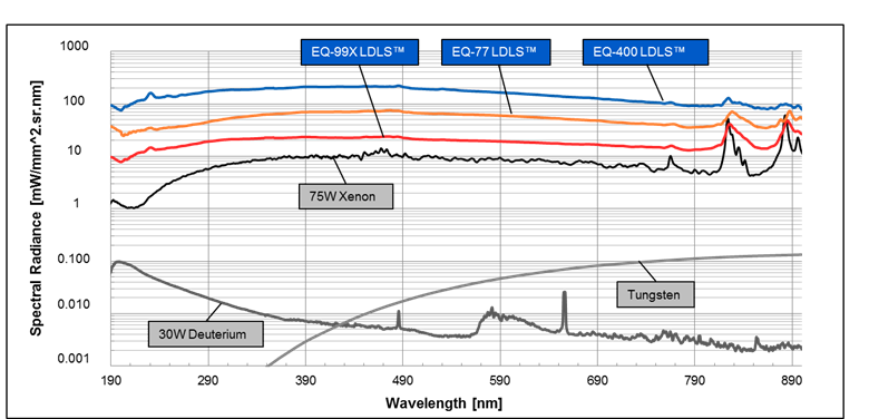
[1], resulting in much higher brightness and smoother emission spectra, Figure 2.
Figure 1.
Operation principles of Laser-driven light sources (LDLS) Figure 2.
Laser-driven light sources (LDLS) spectral radiance performance comparison to conventional broadband light sources. Compared to an electric-discharge plasma in the highest-brightness conventional short-arc Xe lamp (75W) with electrodes (a cathode and an anode), the spectral radiances of LDLS products with 20W, 60W, and 400W laser powers (EQ-99X, EQ-77, and EQ-400, respectively) are one to two orders of magnitude higher near the deep-UV wavelengths. The substantially higher deep-UV emission is due to the higher Xe plasma temperatures in LDLS Xe plasmas when compared with conventional DC short-arc Xe lamp plasmas. The high deep-UV brightness will significantly benefit metrology instrument designs for smaller semiconductor technology nodes. The higher Xe plasma temperatures in LDLS sources also make a broadband spectrum flatter smother in the deep-UV and visible wavelengths, due to higher UV-to-visible radiation ratio.
In an LDLS source, the two electrodes inside the high-pressure Xe bulb only carry a pulse current during plasma ignition. After the ignition, there is zero current going through the electrodes, so there is no direct contact between the high-temperature Xe plasma and the electrodes, so there will not be a deposit of the electrode materials on the inner wall of the fused silica bulb.
Due to their “electrode-less” operation mechanism, LDLS sources have much higher reliability, compared to conventional light sources. Typical for a semiconductor industry application, it is recommended to operate an LDLS product continuously for a one-year period (or 9000 hours of accumulated operation) before performing a Xe bulb replacement as preventive maintenance.
LDLS sources also have better temporal and spatial stabilities compared to DC short-arc Xe lamps. The diode laser output in an LDLS source is stabilized by a precision constant current driver and a closed–loop TEC temperature control circuit. The spatial stability of the plasma position is ensured by a fixed optical system which delivers the laser beam to the plasma.
Due to these desirable features, LDLS products are also used in many other non-semiconductor related applications
[2].
3. Advanced Patterning Metrologies That Use Broadband Light Sources
The semiconductor equipment makers are continuously improving lithography metrology methods and tools to ensure higher accuracy and stability required by the rapid advancement of patterning technology. Metrology tools are used for on-product overlay (OVL) control, inline monitoring, scanner qualification, patterning control, and critical dimension (CD) measurement. The continuously advancing metrology needs for process control and dispositioning of product continue to drive improvements in measurement uncertainty. In addition, there are constant pressures to provide in-situ and in-line measurements that offer higher wafer production throughput. New materials in different process areas add to the challenges faced by lithography metrology.
Metrology methods using broadband light sources are able to obtain more parameters under the same instrument configuration. The widely adopted metrology techniques for CD, overlay, defectivity, and material properties, using broadband light sources, are spectroscopic scatterometry, spectroscopic ellipsometry (SE), and spectroscopic reflectometry (SR)
[3] ,[4].
Scatterometry-based measurement modules provide high performance and cost-effective characterization of overlay error for advanced processes at the 2Xnm/1Xnm design nodes
[6]. Specular spectroscopic scatterometry (SSS) can make direct use of the existing spectroscopic ellipsometry equipment and a UV-visible broadband light source (250nm-800nm) to provide an accurate and non-destructive CD metrology solution
[6] ,[7]. Scatterometry-based metrology for self-aligned quadruple patterning (SAQP) pitch walking using virtual reference has been developed by several groups for 10nm technology nodes and beyond.
Spectroscopic ellipsometry and reflectometry tools are sensitive to many parameters of interest to the thin-film coating process. They provide reliable, high-precision measurements of thin and thick film thickness, refractive index and stress for a broad range of film layers. Models have to be built for the near-surface region to get useful information.
Another actively studied technique for nanostructure metrology is broadband Mueller matrix imaging ellipsometry. LDLS sources were used in many of the research works
[8] ,[9],[10].
In all the metrology techniques discussed above, a high brightness broadband light source is needed. With the help of custom designed optics, a small diameter broadband light beam can be formed from the high brightness light source to illuminate a small targeted area on a wafer to make metrology measurements.
4. End-Point Monitoring for Etching, CVD, and CMP Processes
An automated end-point detection (EPD) is essential for many different wafer processes such as etching, chemical vapor deposition (CVD), and chemical mechanical polishing/planarization (CMP) to ensure that the processes are carefully controlled and consistent. With a proper EPD used in the process, reliable wafer-after-wafer, results are achieved, and device yields can be optimized.
Reflectometry (and interferometry) relies on an external light source which is directed onto the wafer. The reflected light is detected and analyzed. If there is a stop layer with different reflectivity, then there will be a clear end-point signal produced. Typically an EPD sensor head is tool specific and consists of a broadband light source and a spectroscopic light detector.
Scanning white-light interferometry (interference microscopy) is a technique especially suited for CMP surface topography applications due to its ability to measure wafer die level topography with its large (~mm) area field of view high spatial resolution
[11].
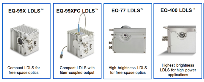
5. LDLS Products for Optical Metrology and Inspections
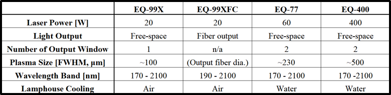
Energetiq’s LDLS products suitable for lithography optical metrology and inspection application are shown in Figure 3. The main parameters for the LDLS products are listed in Table 1.
Figure 3.
Laser-driven light sources models with different laser power and design features. A standard feature for LDLS models with free-space output is that the output light covers 170nm - 2100nm when using UV-grad fused silica windows. For users preferring no nitrogen purging of their optical path, and only needing radiation above 200nm, special windows are available to cut off light output under 200nm eliminating most of the ozone generation along the light path. For applications where only radiation above 320nm is needed, BK-7 glass windows can be used to completely prevent any ozone generation along the light path. The variation of ozone concentration along an optical light path can introduce signal noise in the 220nm to 280nm band due to strong light absorption at that wavelength band by ozone
[12].
Table 1. Main parameters of the four LDLS products.
For users who prefer the flexibility of an optical fiber light output, the EQ-99XFC is an option. The EQ-99XFC lamphouse has an FC/PC connector for an output fiber attachment. There is an off-axis-ellipsoid (OAE) mirror inside the EQ-99XFC lamphouse to collect radiation from the Xe plasma and to focus the beam to the input end of the optical fiber. A fiber core diameter of 200um to 600um will have the best match to the focused spot from the OAE mirror. Output fibers with core diameter smaller than 200μm will be overfilled so output flux will be lower. For fibers larger than a 600μm core diameter it will be underfilled so there is no flux gain while fiber output brightness is reduced. Due to its higher brightness and smaller plasma size, compared to a conventional short-arc Xe lamp, an LDLS source can have more light flux couple into a smaller diameter fiber in reflectance spectroscopy study of plasma-induced physical damage on Si substrate
[13].
LDLS products have been used by metrology equipment researchers and manufacturers for several years and have proven sufficiently valuable that they represent the current industry standard.