

China's IC industry has been flourishing in recent years, huge market demand together with government investments are the major driving forces for this development. The status and development momentum of the Chinese IC industry also attracted wide interest and attention of international counterparts. A group of domestic IC experts are invited by the JoMM to write a series of articles about China's IC industry, including the history, current status, development, and related government policies. Information in these articles is all from public data from recent years. The purpose of these articles is to enhance mutual understanding between the Chinese domestic IC industry and international IC ecosystem. The following article is the second one of this series, the status quo of China's IC industry. The IC industry chain is very long including design, manufacturing, special equipment, materials, packaging and testing. The article series are arranged in accordance with this scope.
In recent years, China's semiconductor equipment industry has made considerable progress, some key equipment have been developed, achieving a revolutionary breakthrough. Meanwhile, a great number of domestic equipment have been applied to large mass production lines, indicating new progress in industrialization.
From the policy perspective, the state has continuously introduced policies to support the localization of the semiconductor industry, and has invested more than 100 billion yuan to boost the development of the semiconductor industry chain since 2014. "Made in China 2025" provides a clear roadmap for the localization of semiconductor equipment: by 2020 the localization rate of 90 ~ 32 nm process equipment target is 50%, the localization rate of 90 nm lithography scanner and key equipment of packaging and testing is 50%; by 2025 the localization rate of 20 ~ 14nm process equipment reaches 30%, with the realization of lithography immersion scanner localization. Throughout China’s semiconductor equipment market, it has long been monopolized by international giants such as Applied Materials and Colin. Among the top 10 semiconductor equipment manufacturers, the United States companies occupy nearly half of the list, while China depends heavily on the import for a long time. To overcome this situation, China’s domestic semiconductor equipment manufacturers rose gradually and obtained considerable progress. It is reported that the main key equipment for 8-inch manufacturing, including etch, ion implantation, film growth, oxidation furnaces, cleaning, single crystal growth, CMP, packaging and others have achieved basic domestic supporting capability. The functionality can satisfy the customer's fundamental demands.
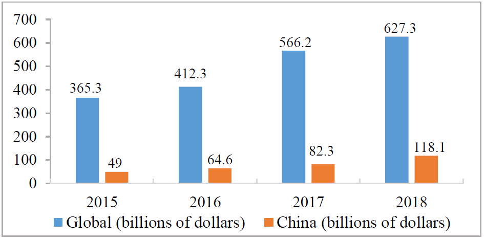
International Semiconductor Industry Association (SEMI) released its mid-year forecast at the annual SEMICON West exhibition: global sales of semiconductor manufacturing equipment are expected to reach $62.73 billion in 2018, a jump of 10.8% from one year earlier, surpassing last year's high record of $56.6 billion. China's semiconductor manufacturing equipment sales in 2017 were $8.23 billion and are expected to reach $11.81 billion by 2018. Another front-end component of the market including manufacturing and mask equipment is expected to grow by 12.3% to $2.8 billion. The packaging section is expected to grow 8.0% to $4.2 billion in 2018, and the semiconductor testing equipment is expected to grow 3.5% to $4.9 billion. China is forecasted to rise to the second place for the first time in 2018 for the semiconductor manufacturing equipment market. China will lead by its growth of 43.5%, followed by the rest of the world (mainly Southeast Asia), with a growth rate of 19.3%, Japan-32. 1%, Europe-11. 6%, North America-3.8% and Korea-0.1%.
2. A Survey of Domestic Integrated Circuit Special Equipment
IC manufacturing is divided into wafer manufacturing and processing. Wafer manufacturing refers to the use of SiO2 as raw materials to produce monocrystalline silicon, which needs smelting furnace, CVD equipment, single crystal furnace and slicer equipment; the wafer processing refers to the process of making logic circuit on wafers, including coating, lithography, development, etching, ion implantation and so on, it also needs PECVD, LPCVD and diffusion furnace. IC packaging and testing are the back end of IC production, they include wafer thinning, cutting, patch, lead bonding, packaging, testing and other processes. Table 1 shows the equipment used in various stages of IC manufacturing. According to SEMI’s estimate, the investment of equipment accounts for about 80% of the whole integrated circuit production line, indicating the importance of equipment in the manufacturing.
| Module | Main process | Required equipment |
| Diffusion | Oxidation, RTP, Laser thermal annealing | Nitriding furnace, RTP equipment, Laser thermal annealing equipment |
| Lithography | Gluing, Photolithography, Develop | Glue spreader, Developer, Mask Aligner |
| Etch | Dry etch, Wet etch, Peeling, Cleaning | RIE, Wet etching equipment, Plasma stripper, Cleaning equipment |
| Ion implantation | Ion implantation, Peeling, Cleaning | Ion implanter, Plasma stripper, Cleaning equipment |
| Film growth | CVD, PVD, RTP, ALD, Cleaning | CVD equipment, PVD equipment, RTP equipment, ALD equipment, Cleaning equipment |
| Polishing | CMP, Wafer scrubbing, Cleaning, Measure | CMP equipment, Plate painting equipment, Cleaning equipment, Measuring equipment |
| Metallization | PVD, CVD, Electroplating, Cleaning | PVD equipment, CVD equipment, Electroplating equipment, Cleaning equipment |
| Back thinning | Incoming material inspection, Sticking film, Back grinding, Dry film stripping | Test equipment, Splitting equipment, wafer grinder, Die-demounter |
| Die saw | Install, Cutting, Cleaning, Optical Detection | Cleaning equipment, AOI |
| Die attach | Die attach, Paste, Curing | Chip mounter, Oven |
| Wire bond | Wire bond, Cleaning, Detection, Injection molding , Marking, Baking, electroplating, Annealing | Lead stitching equipment, Plasma dry cleaner, AOI, Injection molding equipment, Laser marker, X-Ray Equipment, Electroplating equipment, Annealing furnace |
| Trim & Form | Trim, Form, Optical detection | Trim & Form equipment, AOI, Test equipment |
| Test | Test | Test equipment |
Although there is gap between China and the international leaders, there are still some domestic outstanding enterprises, such as NAURA, a leading equipment manufacturer; AMEC which made a breakthrough in etching equipment; packaging & testing field leading company Changchuan Technology; high-purity process system provider PNC Solutions; single crystal growth equipment provider JingSheng Technology and so on.
| Equipment | Application | Foreign Manufacturer | DomesticManufacturer |
| Diffusion (oxidation) furnace (VDF) | Provide oxidation atmosphere for semiconductor materials and realize the oxidation process of semiconductor prediction design. | Thermco(UK), Centrotherm Thermal Solutions GmbH Co.KG(Germany) | NAURA, Qingdao Furunde, 48th of CETC, Qingdao Xuguang, 45th of CETC |
| Vapour epitaxial furnace | Provide a special process environment for the vapor phase epitaxy to grow thin layer crystals on single crystals and prepare for the functionalization of single crystal substrates. | CVD Equipment(USA), GT(USA), Soitec(France), AS(France), ProtoFlex(USA), Kurt J.Lesker(USA), Applied Materials(USA) | 48th of CETC, Sunred, Hefei Kejing, Beijing Jinshengweina, Jinan Liguan |
| LPCVD | A thin film is formed by chemical reaction on the substrate surface with the addition of reactants and other gases. | Hitachi( Japan) | Chijian Tech, 48th of CETC, 45th of CETC, Beijing Instrument Factory, Shanghai Machinery Factory |
| Magnetron sputtering | High rate sputtering of target atoms or molecules to form thin films on substrates by magnetic field. | PVD(USA), Vaportech(USA), AMAT(USA), Hauzer(Holland), Teer(USA), Platit(Switzerland), Balzers(Switzerland), Cemecon(Germany) | Beijing Instrument Factory, SKY Technology Deve-lopment, Chengdu Nanguang Industry, 48th of CETC, Corey Equipment, Shanghai Machinery factory |
| Mask Aligner | Transfer the mask pattern onto photoresist, and temporarily "copy" the device or circuit structure onto the wafer. | ASML(Netherlands) , Lam Research(USA), Nikon(Japan), Canon(Japan), ABM(USA), SUSS(Germany), MYCRO(USA) | 48th of CETC, 45th of CETC, Shanghai Machinery Factory, Chengdu Nanguang Industry |
| Etcher | The chemical reaction etching and physical impact are realized by applying high frequency voltage and ion high speed impact pattern, and the semiconductor processing is realized. | Evatech(Japan), NANOMASTER(USA), REC(Singapore), JuSung(Korea), TES(Korea) | AMEC, Beijing Instrument Factory, NAURA, Chengdu Nanguang Industry, 48th of CETC |
| Ion implanter | Doping the area near the Surface of Semiconductor | Varian SemiconductorEquipment(USA), CHA(USA), AMAT(USA) | Beijing Instrument Factory, 48th of CETC, Chengdu Nanguang Industry, Shenyang Fangji Machinery, Shanghai Silicon Microelectronics |
| CMP | The abrasive body (semiconductor) was ground and polished by the combined action of mechanical grinding and chemical liquid dissolution "corrosion". | Applied Materials(USA), Novellus Systems(USA), Rtec(USA) | Lanzhou Lanxin Hi-tech Industry, Alitesemitech |
| Equipment | Equipment function | Foreign manufacturer | Domestic manufacturer |
| Wafer thinning equipment | The thickness of the wafer is thinned by polishing. | DISCO(Japan), G&N(Germany), OKMOTO(Japan), Camtek(Israel) | Lanzhou Lanxin Hi-tech Industry, FangDa Ginder, Shenzhen Jinshili Equipment |
| Wafer scriber | Cuts a wafer into small pieces. | OEG(Germany), DISCO(Japan) | 45th of CETC, Beijing Kechuangyuan, Shenyang Institute of Instrument and Instrument Technology, Huisheng Electron, Lanzhou Lanxin Hi-tech Industry, HANS LASER |
| Die Bonder | Connect the pad on the semiconductor chip to the pad on the pin with a conductive wire. | AIITEK(USA), TPT(Germany), FK(Austria), UNISEM(Malaysia) | 45Th of CETC, Beijing Chuanshijie, UNISEM |
| Equipment | Equipment function | Foreign manufacturer | Domestic manufacturer |
| Test equipment | Performance test of electrical parameters for various MOS transistors, diodes, IGBT and other power devices and circuits. | Teradyne(USA), Advantest(Japan), Agilent(USA), Epson(Japan), HonTech(Taiwan) | ChangChuan Technology, ACCOTEST, Cascol |
| Wafer scriber | Automatic sorting of Integrated Circuits with different packages. | ChangChuan Technology | |
| Probe station | Electrical test through the pad contact between the probe and the semiconductor device, determine whether the performance index of the semiconductor meets the design performance requirement. | QA(USA), Ingun(Germany), MicroXact(USA), Ecopia(Korea), Leeno(Korea) | 45Th of CETC, NAURA, Ningbo Rooko Instrument, WAROM |
2.1.
NAURA
As the leading domestic equipment company, NAURA delivers four kinds of products: semiconductor equipment, vacuum equipment, lithium electric equipment and electronic components. Its semiconductor equipment covers plasma etching equipment, PVD, CVD, oxidation furnace and other production line core equipment. The 28nm PVD equipment of NAURA has been implemented in the SMIC production line, and the etching, annealing and CVD equipment for 14nm process have also reached the stage of process verification.
NAURA has strong capability in oxidation furnace, etching equipment, film deposition equipment and cleaning equipment. On November 30, 2017, the 12-inch vertical oxidation furnace THEORISO302MoveIn YMTC production line developed by NAURA microelectronics, a subsidiary of NAURA, was applied to 3D NAND Flash process and expanded the application field of domestic vertical oxidation furnace. A silicon etching equipment for 14nm process was developed in 2016 and is currently under verification in SMIC's 14nm process. In November 2017, China's first metal etching equipment for 8-inch wafers was successfully applied in SMIC's production line. Batch shipment has been realized in 28nm grade PVD equipment and monolithic annealing equipment. Many kinds of production equipment such as 14nm ALD, ALPVD, LPCVD, HMPVD are in the process of production line verification. The self-developed 12-inch single-chip cleaning equipment products are mainly used in the integrated circuit chip process. After the successful acquisition of Akrion on August 7, 2017, the NAURA microelectronics cleaning equipment product line will be replenished, forming a product line covering integrated circuits, advanced packaging, power devices, micro-electromechanical systems, semiconductor lighting and other semiconductor areas of 8-inch and 12-inch cleaning product lines.
2.2.
AMEC
AMEC was founded in 2004 by Dr. Yin Zhiyao who worked for Applied Materials for 13 years, specializing in the development of plasma etching equipment. AMEC is the leading high-end chip equipment enterprise in China, and was the first to be invested by the national large fund since established. Its chip dielectric etching equipment has entered the world's top enterprise TSMC’s 10 nm production line, and accounted for more than 50% of SMIC's new procurement. In 2015, the U.S. Commerce Department lifted restrictions on the export of etching equipment to China because of AMEC's "considerable quantity and equal quality" etch equipment products. The company is expected to achieve leapfrog growth and become a leading domestic semiconductor industry company.
AMEC is also strong in the dielectric etching equipment, through-silicon via etching equipment and MOCVD for LED. At present, the dielectric etch equipment can achieve 22nm and below, 14nm model is also in the production line to be verified, while the joint study of 5nm is being promoted. Through-silicon via etching equipment is mainly used in TSV advanced packaging of integrated circuit chip. AMEC's MOCVD has reached the advanced level in the world, and it has realized the import substitution of American VEECO and German Aixtron products. The customers are leading chip manufacturers such as San'an Optoelectronics. As of October 2017, its MOCVD equipment PrismoA7 model shipments have exceeded 100 sets.
2.3.
ChangChuan Technology
ChangChuan Technology has always focused on the field of semiconductor testing equipment, the main product line includes testing equipment and sorting equipment, and its main customers include Hua Tian, JCET, Silan microelectronics and other packaging & testing and manufacturers. The company has developed the high precision voltage and current source control and measurement technology, high current power supply high energy pulse control and testing technology and other core technologies, it has gained advanced technologies that are comparable with Europe and the United States competitors.
2.4.
ACMR
Originally founded in Silicon Valley, ACMR was introduced into Zhangjiang, China in 2007, mainly producing cleaning equipment, copper plating equipment and other products. Its ultrasonic cleaning technology overcame the technological difficulties brought by the development of chip manufacturing process. ACMR products are adopted by SMIC, Korea Hynix and other well-known semiconductor manufacturers, and ACMR gained support from "02 National Special Project”. ACMR went NASDAQ IPO on November 3, 2017, becoming one of domestic equipment manufacturers pushing into overseas markets.
ACMR has strong capability in the field of cleaning equipment. Its SAPS technology can be applied to the silicon wafer cleaning of the 65nm process, and the TEBO technology can cover the process of the FinFET, DRAM, 3DNAND, and the products have been applied to the mass production line in Shanghai Huali Microelectronics. In addition, the company invested $30 million in Hefei in May 2017 to set up a research and development center in order to develop DRAM technology with Hefei Changxin and GigaDevice.
2.5.
PIOTECH
PIOTECH is a high-tech enterprise established by overseas technical experts in April 2010, dedicated to the development and production of the world's leading special film equipment for the integrated circuit industry. The company has launched a 12-inch PECVD, ALD, 3D NAND series product line, and undertook two national scientific and technological key projects with the solid support from the national fund. In 2013, PIOTECH’s 12-inch PECVD passed the SMIC product line test, and in October 2017, the company's equipment in Beijing SMIC International mass production exceeded millions of move, which is a significant milestone. PIOTECH’s industrial manufacturing base has a maximum throughput capacity of 350 sets of equipment per year and annual revenue of 5 billion yuan.
2.6.
CETC
CETC is competitive in the field of ion implantation equipment and CMP. The 45-22nm low energy large beam ion implantation equipment was launched in 2016 and verified in SMIC production line in 2017, improving the localization rate of SMIC ion implantation equipment. On November 21, 2017, CETC completed internal testing of its self-developed 200mm CMP commercial equipment and sent to SMIC Tianjin for in-line verification. This was the first time that domestic 200mm CMP equipment was implemented in a large integrated circuit production line.
2.7.
SMEE
SMEE is the only domestic company engaged in the research and manufacture of lithography equipment. At present, its lithography equipment for mass production can only achieve 90 nm, and there is still a big gap to the mainstream 65nm node and below. However, the packaging lithography tools can be largely used as long as the resolution requirement is 1-2 microns. SMEE’s 500 series stepper is targeted at the IC back end packaging and MEMS/NEMS manufacturing applications, and takes over 80% share of the domestic market.
Acknowledgments
We would like to extend appreciation to the graduate students: Weichen Liu, Tianyang Gai, Cheng Guo, Pengzheng Gao from the Institute of Microelectronics of Chinese Academy of Sciences (IMECAS) and Lei Qu, Xiaoting Li from North China University of Technology for their contribution of contents.
