2.1. Yangtze Memory Technology Corp. (YMTC)
In July 2016, Tsinghua Unigroup, National Integrated Circuit Industry Investment Fund, Hubei Integrated Circuit Industry Investment Fund, and Hubei Science & Technology Investment Group Co., Ltd established YMTC. According to statistics, the total investment of YMTC is about 160 billion yuan. Among them, Tsinghua Unigroup accounted for 51.04% of the shares [3].
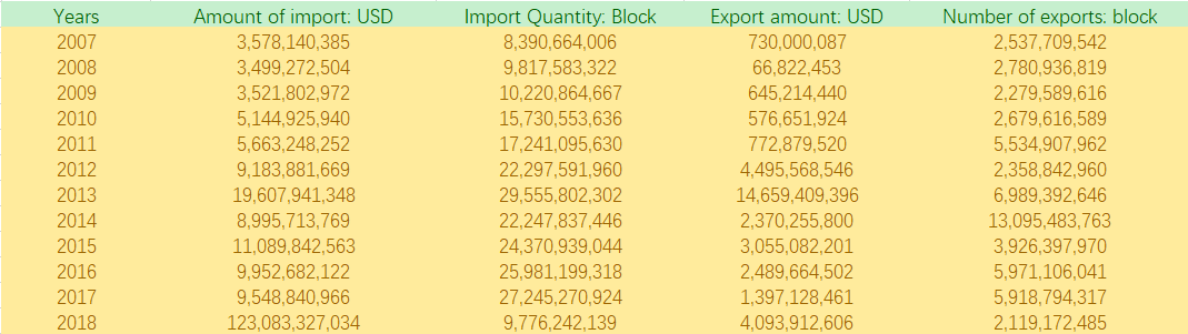
In December 2016, the national memory base with YMTC as the main body officially started construction, including three 3D NAND Flash Fab plants with the most extensive clean room in the world, one headquarters R&D building and several other supporting buildings. It is expected that after the project is completed, the total production capacity will reach 300,000 wafers per month, and the annual revenue will exceed 10 billion dollars. Relying on the existing 12-inch advanced integrated circuit technology research and development and manufacturing capabilities of Wuhan Xinxin Manufacturing Co., Ltd. (XMC), the independent R&D and international cooperation are carried out in parallel, YMTC has successfully developed China's first 3D NAND flash memory chip in 2017. With the mass production of 32-layer NAND Flash of YMTC in 2018, China's flash memory chips have finally achieved a breakthrough. However, due to the fact that the technology is quite different from the global mainstream technology, it will not affect the market.
In contrast, in 2019, YMTC officially announced the mass production of 64-layer 256 Gb TLC 3D NAND Flash based on the self-developed Xtacking architecture, remarkably it can bring competition to the current middle- and low-end market. Note that, this flash memory meets the mainstream market application requirements such as solid-state drives and embedded storage. Compared with the 64/72-layer 3D NAND flash memory currently available in the industry, it has higher storage density. This is mainly attributing to the Xtacking architecture independently developed by Yangtze River Storage. At present, NAND flash memory mainly uses two I/O interface standards, in which the first standard refers to Intel/Sony/SK Hynix/Group/Western Digital/Micron's ONFi. The latest ONFi 4.1 specification released in December last year can deliver I/O interface maximum speed up to 1200MT/s (1.2Gbps). The second standard is Samsung/Toshiba's Toggle DDR, with I/O speed up to 1.4Gbps. However, most NAND suppliers can only provide I/O speed of 1.0 Gbps or lower. The Xtacking architecture of YMTC has successfully increased the speed of the I/O interface to 3Gbps, which is comparable to the I/O speed of DRAM DDR4.
In terms of production capacity, according to the plan, the capacity of 64-layer 3D NAND flash memory of Yangtze Storage by the end of 2020 is expected to increase to 60,000 wafers per month. In 2020, YMTC will skip the 96-layer stack and go directly to the 128-layer stack, striving to shorten further the gap with companies such as Samsung and Toshiba.
According to Chen Jiewei, research associate of DRAMeXchange [4], a researcher of Jibang Technology, the Changjiang Storage Chengdu Plant is expected to be put into operation in the Q2 2020, when it may have a production capacity of 5,000 wafers per month. By the Q4 2020, the production capacity can climb to 20,000 wafers per month. The current capacity of the Wuhan factory of YMTC is about 20,000 wafers per month. It is expected to reach 50,000 wafers per month by the Q4 2020. By then, the capacity of the entire 3D NAND Flash of Yangtze Storage will reach 70,000 wafers per month. It is already close to Intel's 85,000 wafers per month production capacity. However, compared with Samsung's production capacity of 470,000 wafers per month, there is still a considerable gap. It only accounts for 4.6% of the global 3D NAND Flash production capacity. However, Chen Weiwei expects that as Yangtze Storage's new 3D NAND Flash production capacity continues to increase, it is expected that by 2023, YMTC's share of global 3D NAND Flash production capacity will increase to 10.8%, in order to catch up with Intel (6.6%) and Micron (10.3%).
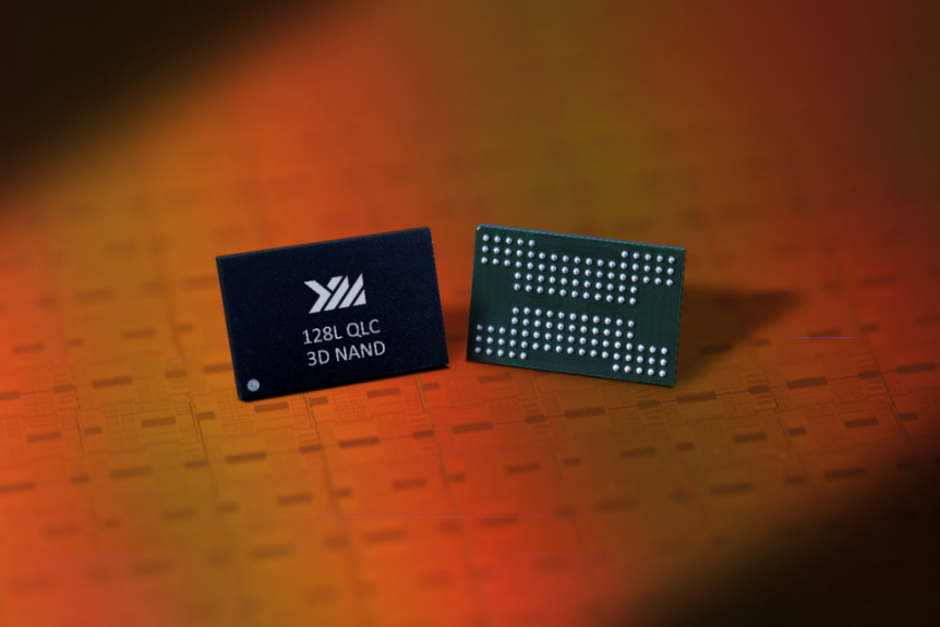
On April 13, 2020, YMTC announced that its 128-layer QLC 3D NAND flash memory (model: X2-6070) has been successfully developed and has been verified on terminal storage products such as SSDs of multiple controller manufacturers. X2-6070 is the industry's first 128-layer QLC 3D NAND flash memory with the highest storage density per unit area, the highest I/O transfer speed and the highest capacity of single NAND flash memory chip. Also released this time are 128-layer 512Gb TLC (3 bit/cell) flash memory chips (model: X2-9060) to meet the needs of different application scenarios.
Figure 2.
128L QLC 3D NAND. Chang Yi, Senior Vice President of Yangtze Storage Markets and Sales, said: "As a newcomer in the flash memory industry, YMTC has achieved a leap from 32 layers to 64 layers to 128 layers in just three years. The cohesion of people's sweat is also the result of a collaboration between the upstream and downstream of the global industrial chain. With the advent of the Xtacking 2.0 era, YMTC has the determination, strength, and ability to create a new business ecology, so that our partners can fully Use their advantages to achieve mutual benefit and win-win."
As a semiconductor memory enterprise integrating chip design, process development, wafer production and testing, sales and service, YMTC provides advanced storage products and solutions for customers worldwide, which are widely used in mobile communications, computers, data centers and consumer electronics and other fields.
2.2. Fujian Jinhua Integrated Circuit Co., Ltd. (JHICC)
JHICC was established in 2016. It is an advanced integrated circuit manufacturing enterprise jointly established by Fujian Electronic Information Group and Jinjiang Energy Investment Group Co., Ltd [5]. The Jinhua project has been included in the national "Thirteenth Five-Year Plan (2016-2020)", specifically in the important layout of integrated circuit productivity planning, and has achieved support by the national special construction fund which is investment from Fujian Anxin Industrial Investment Fund. The fund was jointly developed and established by the "National Integrated Circuit Industry Investment Fund (commonly known as the Big Fund)" and three levels of government including Fujian Province, Quanzhou City, and Jinjiang City, with a target scale of 50 billion yuan.
In November 2017, the main plant of the 12-inch random access memory (DRAM) production line (Jinhua Project), which was jointly operated by UMC and JHICC, was officially capped. The Fab main plant, with an area of 274,000 square meters, will be put into use in the second half of 2018.
According to the plan, the manufacturing technology work of JHICC is mainly carried out by UMC. The first phase of the overall JHICC project will invest a total of 5.3 billion US dollars and will be officially put into production in the third quarter of 2018. The monthly capacity of inch wafers is expected to reach 60,000 wafers. The company aims to launch a 20-nanometer product finally and plans to complete a monthly production capacity of 240,000 wafers by the fourth phase by 2025.
However, due to the litigation between JHICC and Micron, on October 29 local time in the United States, the United States included JHICC on the list of entities subject to export control [6]. Two days later, UMC also announced a suspension of R&D support for JHICC. So far, Jinhua, Fujian's DRAM has almost stagnated.
At that time, JHICC had 200 semiconductor devices in place and planned to conduct small-scale trial production at the end of the year. It was expected that it would realize volume production at the scale of several thousand wafers by early 2019. It planned to become the first domestic manufacturer of mass-produced DRAM chips soon. However, due to the U.S. ban, many related equipment and technology suppliers stopped supporting.
2.3. GigaDevice Semiconductor Inc.
As a listed company, GigaDevice is the first integrated circuit design company specializing in the design of memory and related chips [7]. Committed to the design and development of various high-speed and low-power memory, high technology, low power consumption, and low cost are its product characteristics. Successfully developed the first Serial Flash product and the first GigaROM product in 2008, breaking the monopoly of foreign countries and filling the domestic gap. In 2012, the monthly sales of Serial Flash products exceeded 70k for the first time, and the production process was advanced to 65nm, serial the market share of flash memory has always remained the first in China.
In October 2019, Gigadevice's new generation of high-speed 8-channel SPI NOR Flash-GD25LX256E won the 2019 14th "China Chip" Excellent Technology Innovation Product Award issued by the China Electronics and Information Industry Development Research Institute. GD25LX256E is the new GD25LX series launched by Gigadevice in 2019. It is also the first domestic high-speed 8-channel SPI NOR Flash product with a maximum clock frequency of 200 MHz and a data throughput rate of up to 400 MByte/s, which is five times that of current products the above.
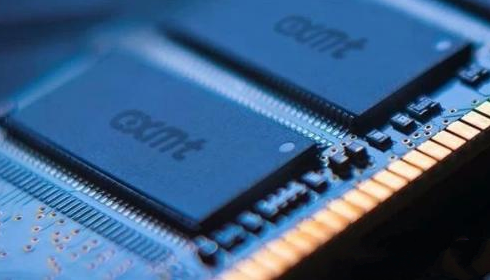
Figure 3.
MCU based on RISC-V core. The main products of Gigadevice are Serial Flash and MCP. The products have the characteristics of high reliability, low power consumption and adaptability to portable applications. The company has advanced production lines from third parties and strong production capacity support. Continuous improvement and production cost control. Products are widely used in handheld mobile terminals, consumer electronics, personal computers and peripherals, networks, telecommunications equipment, medical equipment, office equipment, automotive electronics and industrial control equipment.
2.4. Changxin Memory Technologies Inc (CXMT).
Founded in May, 2016 in Hefei, Anhui, CXMT is an integrated design and manufacturing company specializing in dynamic random-access memory (DRAM) [8]. CXMT has already put its first 12-inch wafer fab into production. DRAM products are used in a wide range of fields, including mobile devices, computers, servers, artificial intelligence, virtual reality, and Internet of Things, enjoying tremendous and growing market demand.
In 2017, through cooperation with Qimonda, Changxin Memory has collected more than 10 million DRAM-related technical documents and 2.8TB of data, which is also one of the original DRAM technology sources of Changxin Memory.
After several years of research and development, on September 19, 2019, Hefei Changxin Memory officially announced the mass production of the independently developed 8Gb DDR4 chip based on the 19nm process.
According to the plan, Changxin Memory Hefei 12-inch fab is divided into three phases. The first phase of full-load production capacity is 120,000 wafers. It is expected to be implemented in three phases. The first phase will complete 40,000 wafers per month, which is currently 20,000 wafers, reaching 40,000 wafers at the end of the first quarter of 2020. Planning and construction of the second phase of the project will begin in 2020, and the development of 17nm process DRAM will be completed in 2021.
From the current situation and planning of Changxin Memory, although it has already achieved mass production of 8Gb DDR4, its production capacity is still minimal. Even if the production capacity of 40,000 wafers per month in the first phase of next year is achieved, compared with the total volume of more than 1.3 million wafers per month that the top three manufacturers in the world can achieve in the fourth quarter of next year, it is still It is a stalemate. However, it is foreseeable that with the continuous improvement of Changxin Memory technology and production capacity, it is expected to occupy an essential place in the global DRAM market in the future.
Changxin aims to comply with the national strategy of accelerating the development of the integrated circuit industry, relying on the strong support of the Hefei municipal government and industrial capital, introducing first-class talents and process technology, concentrating on research and development of its intellectual property, and committed to becoming the first 12-inch in China Professional storage IDM enterprise.
The company gathered leaders in the integrated circuit industry, experts in R&D, design and manufacturing, as well as an international management team. Adhering to the concept of continuous, honesty and integrity, and actively cultivating outstanding local talents, we are determined to become a model company of "Created in China" with cutting-edge technology development capabilities and process manufacturing capabilities. The company has a total investment of 8 billion US dollars in the first phase and plans to complete the construction of the plant in the third quarter of 2017 and achieve formal production in 2018.
At present, the Hefei Changxin 12-inch memory wafer manufacturing base is in the stage of accelerating construction. Once the project is officially put into production, it is expected to account for about 8% of the global DRAM market share, thereby filling China's DRAM memory in the domestic market Whitespace.
2.5. Tsinghua Unigroup
The company's leading products include surface treatment of electronic chemicals and w Tsinghua Unigroup is the second-largest integrated circuit high-tech enterprise in China after Huawei, and it has made massive investment in order to lead the domestic storage chip industry [9]. Since 2016, Tsinghua Unigroup has started construction of memory chip and memory manufacturing plants with a total investment of nearly 100 billion U.S. dollars in Wuhan, Nanjing, and Chengdu, which has initiated Tsinghua Unigroup's grand plan in the chip manufacturing industry over the next ten years.
In July 2016, Tsinghua Unigroup, National Integrated Circuit Industry Investment Fund, Hubei Integrated Circuit Industry Investment Fund, and Hubei Ketou jointly established the YMTC based on Wuhan Xinxin, thus forming a controlling stake in YMTC. The total investment to YMTC will be more than 24 billion U.S. dollars. It is also one of Tsinghua Unigroup's most significant investment projects to date.
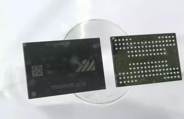
Figure 5.
64G 3D NAND Flash. According to the data, Tsinghua Unigroup began to deploy DRAM as early as 2015. Firstly, Gao Qiquan was recruited to join Tsinghua Unigroup. At the same time, Unigroup Guoxin Microelectronics acquired the company founded by Ren Qiwei's team (now Xi'an Tsinghua Unigroup Guoxin). The predecessor of the Ren Qiwei team was Qimonda's Xi'an R&D Center. The Ren Qiwei team has been engaged in DRAM research and development. The current team number is about 500. According to the disclosure by Tsinghua Unigroup Gowri's annual report, the team's DRAM product sales revenue is about 500-600 million yuan, its products are designed by themselves, and manufactured by foundry abroad. In 2015, Tsinghua Unigroup also tried to enter the field of DRAM and 3D NAND through the acquisition of Micron, but the acquisition of Micron was rejected by the U.S. government thus failed to fulfil its wish.