Archive Versions 1 Vol 3 (2) : 20030202 2020
Download
High-Pressure Oxidation on Ge: Improvement of Ge/GeO2 Interface and GeO2 Bulk Properties
: 2020 - 01 - 23
: 2020 - 06 - 29
1773 32 0
Abstract & Keywords
Abstract: On the basis of thermodynamic and kinetic consideration of Ge-O system, high-pressure oxidation (HPO) on Ge was proposed to suppress the GeO desorption during the thermal oxidation and significant improvements of Ge/GeO2-based gate stacks have been achieved. It is found that the post oxidation annealing at lower temperatures is helpful to passivate the interface defects at the Ge/GeO2 stack generated by the conventional thermal oxidation, while the high-quality GeO2 bulk properties can only be achieved by HPO that grows GeO2 film at high temperatures without the GeO desorption. This paper reviews the advantage of HPO on the formation of Ge/GeO2 stacks in terms of Ge/GeO2 interface and GeO2 bulk properties.
Keywords: High-pressure oxidation; Ge oxidation; High mobility channel; Ge/GeO2 interface; Interface trap density
1.   Introduction
Germanium (Ge) has attracted much interest in terms of application to high mobility channel devices due to its more symmetric and higher carrier mobilities than Si, which could enable us to boost the driving current of transistors. Recently, high electron mobility in Ge n-MOSFETs exceeding the Si universal mobility have been reported [1-6], and the key technology for high performance Ge CMOS is how to effectively improve the Ge gate stacks. It is found that interface passivation of near the conduction band edge is more problematic, which limits the electron mobility in Ge n-MOSFETs. Both high electron and hole mobilities in Ge MOSFETs have only been achieved in Ge/GeO2-based gate stacks [5-8], and GeO2 has received a great deal of attention as an interfacial layer of Ge gate stack. It has been reported that the degradation of electrical properties of Ge/GeO2-based gate stacks is attributed to the GeO desorption at the Ge/GeO2 interface [9]. After that, extensive research efforts for Ge interface passivation have been focused on the mild oxidation. Several oxygen passivation methods of Ge/GeO2 interface for reducing the interface trap density (Dit) have been successfully demonstrated [10-15], where the relatively low temperature (below 450oC) is employed to avoid GeO desorption. However, since the stoichiometric oxide layer is generally formed by high temperature oxidation, these approaches raise the question of whether GeO2 bulk properties and reliability are good enough to meet the requirements of electronic device.
On the basis of thermodynamic and kinetic consideration of Ge-O system, the high-pressure oxidation (HPO) on Ge was proposed to suppress the GeO desorption during the thermal oxidation and significant improvements of Ge/GeO2-based gate stacks have been achieved [16]. In this paper, the advantage of HPO on the formation of Ge/GeO2 stack is reviewed in terms of Ge/GeO2 interface and GeO2 bulk properties.
2.   Ge/GeO2 Interface Passivation
To study the electrical properties of Ge/GeO2 stacks, MOSCAPs with Ge/GeO2 stacks were fabricated. Ge (100) wafers were chemically cleaned using methanol, HCl, H2O2+NH4, and dilute HF solution in sequence before the thermal oxidation, in which HPO was carried out in a specialized furnace in a wide range of temperature and O2 partial pressure (PO2). Note that PO2 in this work is defined at room temperature before increasing the furnace temperature, and that the actual O2 pressure in the furnace during the oxidation should be higher than the PO2. After thermal oxidation, Au and Al were deposited by vacuum evaporation for the gate electrode and substrate contact of MOSCAPs, respectively.

(a)


(b)

Figure 1.   (a) Bidirectional C-V characteristics of p-type MOSCAPs with Ge/GeO2 stack grown by APO at 550oC for 15 min. A large hysteresis and frequency dispersion are observed, indicating that a huge amount of interface and bulk traps are generated by the conventional thermal oxidation. (b) Schematic of Ge/GeO2 stack grown by APO. Ge oxidation and GeO desorption occur simultaneously, resulting in the interface and bulk defects in Ge/GeO2 stack.
Figure 1(a) shows bidirectional capacitance-voltage (C-V) characteristics of p-type MOSCAPs with Ge/GeO2 stack grown by atmospheric-pressure oxidation (APO, PO2 = 1 atm) at 550oC, where a large hysteresis and frequency dispersion are observed. It is inferred that a huge amount of interface and bulk traps are generated during a conventional thermal oxidation. Figure 1(b) shows a schematic of Ge/GeO2 stack grown by APO. Under the APO condition, the Ge oxidation and GeO desorption occur simultaneously, resulting in the interface and bulk defects in Ge/GeO2 stack. The thermodynamic consideration of Ge thermal oxidation is discussed in more detail [16]. Figure 2 shows bidirectional C-V characteristics of p-type MOSCAPs with Ge/GeO2 stack grown by HPO (PO2 = 70 atm) at 550oC, in which nearly no hysteresis and frequency dispersion are observed. The Dit at the Ge/GeO2 interface formed by HPO was estimated by low-temperature conductance method at 200 K and 100 K to avoid the minority carrier response. The minimum value of Dit near the mid gap is about 2e11 eV-1cm-2 without any post oxidation treatment, indicating that the high-quality Ge/GeO2 stack is formed by suppressing the GeO desorption at the Ge/GeO2 interface.


Figure 2.   Bidirectional C-V characteristics of p-type MOSCAPs with Ge/GeO2 stack grown by HPO (PO2 = 70 atm) at 550oC for 15 min. It shows nearly no hysteresis and frequency dispersion and the estimated Dit near the mid gap is about 2e11 eV-1cm-2 without any post oxidation treatment.
Alternatively, GeO desorption can be suppressed by lowering the oxidation temperature since the equilibrium vapor pressure of GeO at the Ge/GeO2 interface is thermodynamically fixed independent of PO2 at a given temperature due to Gibb’s phase rule [17]. The vapor pressure of GeO can be reduced by three orders with a decrease in the annealing temperature from 550oC to 400oC. To investigate the efficacy of suppressing GeO desorption at the interface, the post oxidation annealing in O2 ambient at 400oC for Ge/GeO2 stack grown by APO (550oC, PO2 = 1 atm) is carried out.

(a)


(b)

Figure 3.   (a) Hysteresis of C-V characteristics with APO-grown Ge/GeO2 stacks as a function of post oxidation annealing time. It shows a significant reduction of hysteresis in Ge/GeO2 stack grown by APO, suggesting that Ge/GeO2 interface is effectively passivated by post oxidation annealing at 400oC. (b) Bidirectional C-V characteristics of n-type MOSCAPs with Ge/GeO2 stack grown by APO, followed by post oxidation anneal for 60 min.
Figure 3(a) shows the hysteresis of C-V characteristics as a function of post oxidation annealing time, where the hysteresis is extracted at flat-band voltage. It shows a significant reduction of hysteresis in Ge/GeO2 stack grown by APO, suggesting that Ge/GeO2 interface is improved by post oxidation anneal. The bidirectional C-V characteristics of n-type MOSCAPs with Ge/GeO2 stack grown by APO, followed by post oxidation anneal for 60 min are shown in Figure 3(b). A very small hysteresis and frequency dispersion indicate that the superior Ge/GeO2 interface can be achieved by optimizing the post oxidation annealing even if interface defects are generated by APO. A low temperature conductance method was used to quantitatively estimate the Dit at the Ge/GeO2 interface, as shown in Figure 4, where measurements were carried out in the temperature range of 250 K to 100 K to evaluate a wide range of Dit spectrum in the energy band gap of Ge. It is shown that the minimum value of Dit near the mid gap is below 1e11 eV-1cm-2, which is close to the Ge/GeO2 interface formed by HPO. Thus, it can be inferred that post oxidation annealing can effectively passivate the dangling bonds at the Ge/GeO2 interface generated by GeO desorption during APO. It is worthy to note that post oxidation annealing temperature should be around 400oC to avoid GeO desorption at the interface.


Figure 4.   Energy distribution of Dit estimated by low temperature conductance method in the temperature range of 250 K to 100 K. The minimum value of Dit near the mid gap is below 1e11 eV-1cm-2, which is close to the Ge/GeO2 stack grown by HPO.
3.   GeO2 Bulk Properties
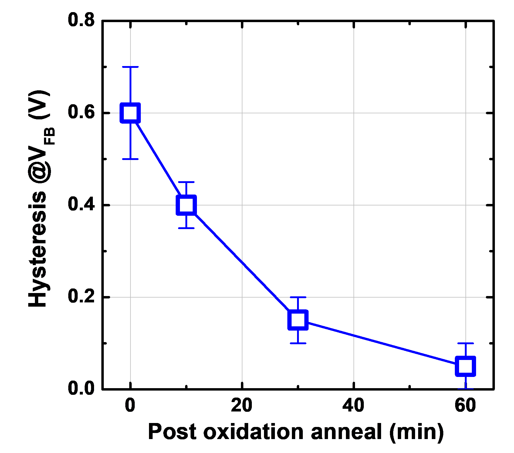
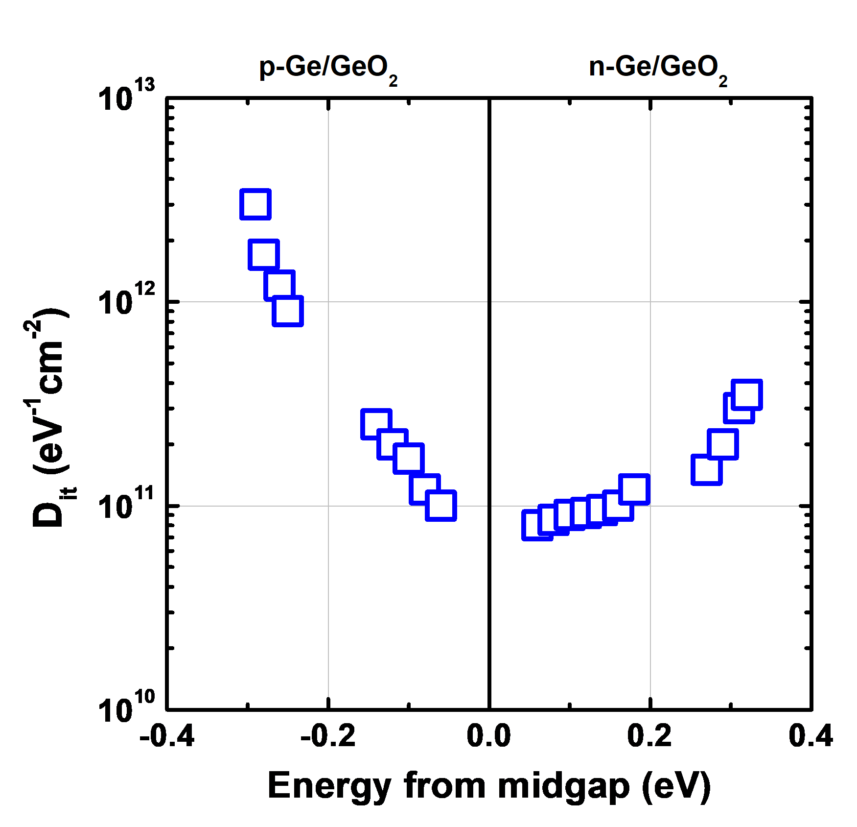
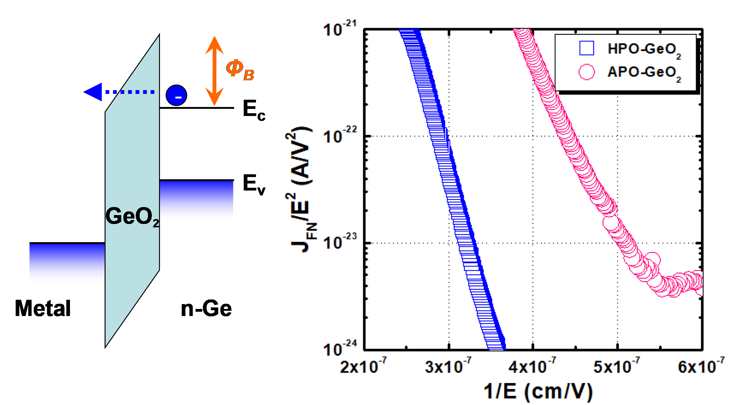
In order to investigate the GeO2 bulk properties in the Ge/GeO2 stack, the same thickness of GeO2 film was thermally grown on Ge (100) wafers by APO and HPO, respectively. For the interface passivation of Ge/GeO2 stacks, the post oxidation annealing at 400oC for 60 min was carried out for both HPO-grown and APO-grown Ge/GeO2 stacks. Since Ge/GeO2 interface properties are superior enough and similar to both HPO-grown and APO-grown Ge/GeO2 stacks with the post oxidation annealing, the influence of Ge/GeO2 interface properties can be excluded from the discussion of GeO2 bulk properties. The conduction band offset (ΦB) is one of the most important factors as the gate insulator to suppress the gate leakage current. In order to extract and compare the ΦB between GeO2 and Ge substrate, both n-type MOSCAPs with APO-grown GeO2 and HPO-grown GeO2 are investigated. Figure 5(a) shows a plot of ln(JFN/E2) versus (1/E), where JFN is the current density and E is the electric field of GeO2, known as the Fowler-Nordheim (F-N) plot. The F-N tunneling current density JFN can be expressed as follows [18]:
,
where and . Here, h is the Planck constant, q is the electron charge, Eox is the electric field in the GeO2, ΦB is the barrier height, m is the free electron mass, and mox is the effective electron mass in the GeO2. Since mox is an unknown factor, mox is assumed to be 0.42m, which is generally accepted as the effective electron mass in the SiO2. If the F-N plot is linear, the intercept of this F-N plot gives A and the slope yields B. The calculated ΦB from above equations is 1.5 eV for HPO-grown GeO2 on Ge and 1.2 eV for APO-grown GeO2 on Ge, respectively. The value of ΦB for Ge/GeO2 stack with APO is well consistent with other report [19], where GeO2 was thermally oxidized at 550oC in 1-atm O2 ambient. Figure 5(b) shows the calculated Φ
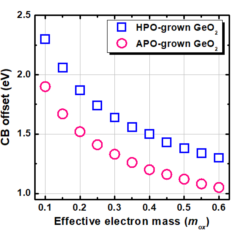
B from F-N plot as a function of mox . It is expected that the ΦB from Ge/GeO2 stack grown by HPO is about 0.3 eV higher than that of Ge/GeO2 stack grown by APO, regardless of mox . This difference of ΦB in the Ge/GeO2 stacks might be originated from bulk defects in the GeO2 film, which is generated by GeO desorption during the conventional thermal oxidation.

(a)


(b)

Figure 5.   
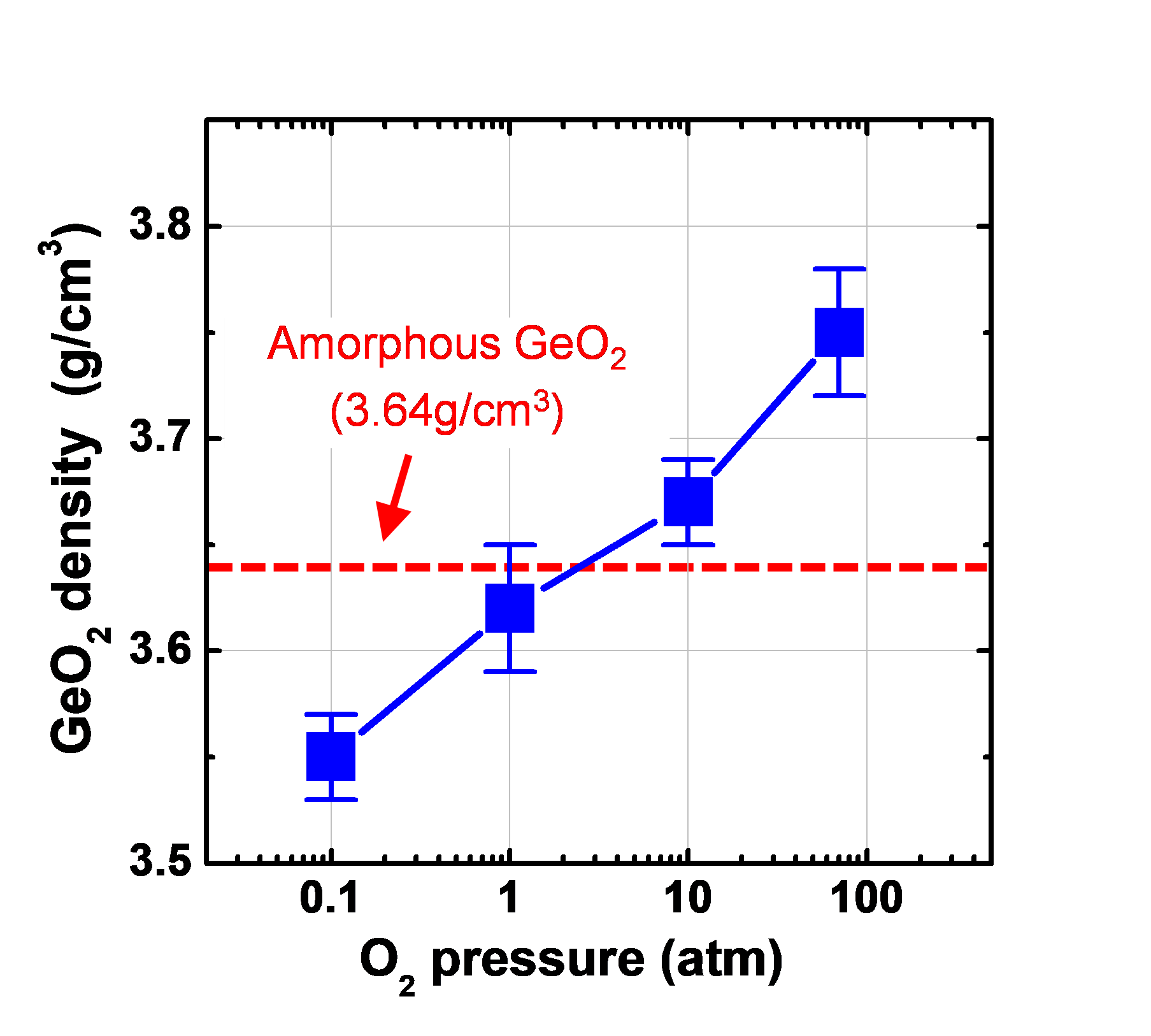
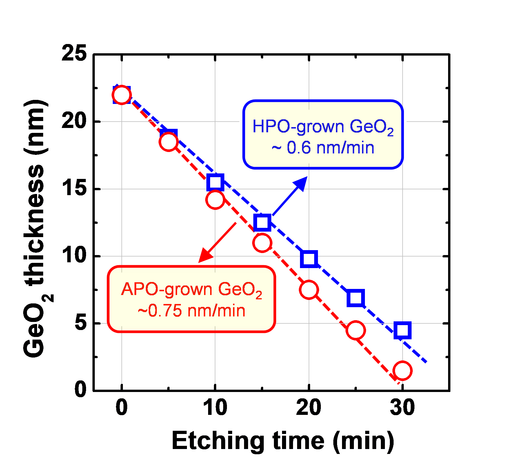
(a) Fowler-Nordheim (F-N) plot for HPO-grown and APO-grown GeO2 on Ge samples, where the thickness of both HPO-grown and APO-grown GeO2 film is 25 nm. Under the assumption that the effective electron mass in the GeO2 is 0.42m, the calculated conduction band offset is 1.5 eV for HPO-grown GeO2 and 1.2 eV for APO-grown GeO2, respectively. (b) Calculated conduction band offset between GeO2 and Ge as a function of effective electron mass in the GeO2. It is expected that the ΦB from Ge/GeO2 stack grown by HPO is about 0.3 eV higher than that of Ge/GeO2 stack grown by APO, regardless of mox .
To further investigate the GeO2 bulk properties, the GeO2 film density was estimated by grazing incidence X-ray reflectometry. Figure 6(a) shows the GeO2 film density as a function of PO2 in the thermal oxidation. It clearly shows that GeO2 film density increases with the increase of PO2. For comparison, the density of amorphous GeO2 film is included [20], which is in good agreement with APO-grown GeO2 film. It is well known that there is a strong correlation between dielectric film density and their wet etch rate. Since GeO2 is water soluble and readily dissolved in deionized water, we prepared the dilute deionized water solution (C2H5OH + H2O) to study the wet etch rate of GeO2 films grown by APO and HPO, respectively. Figure 6(b) shows the wet etch rate of GeO2 film in dilute deionized water solution. As expected from the film density, HPO-grown GeO2 film shows the slower wet etch rate (~0.6 nm/min) than APO-grown GeO2 film (~0.75 nm/min).

(a)


(b)

Figure 6.   
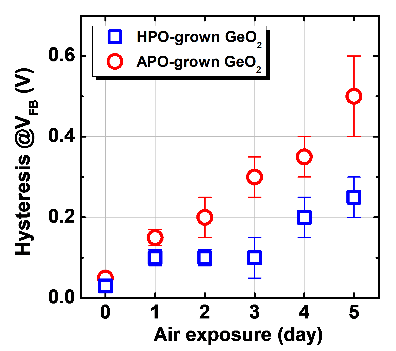
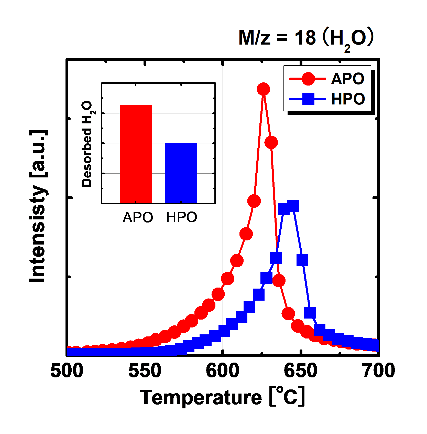
(a) GeO2 film density estimated by grazing incidence X-ray reflectometry as a function of O2 pressure in the thermal oxidation. It clearly shows that GeO2 film density increases with the increase of PO2. (b) Wet etch rate of GeO2 in the dilute deionized water solution. HPO-grown GeO2 film shows the slower wet etch rate than APO-grown one, which is good agreement with PO2 dependence of GeO2 film density.
Since GeO2 film is easily etched in water, a strong influence of moisture absorption in the air on Ge/GeO2 stack is expected. Figure 7(a) shows the hysteresis of C-V characteristics extracted at flat-band voltage as a function of the air exposure time, where Ge/GeO2 stacks were exposed to the air before the gate electrode formation. A clear difference of electrical degradation rate between HPO-grown Ge/GeO2 stack and APO-grown Ge/GeO2 stack against the air exposure is observed. The effects of air exposure on electrical properties in Ge/GeO2 stack in terms of water absorption and hydrocarbons are comprehensively discussed in the literature [21], which is well consistent with our results. After 5-day air exposure, the desorbed H2O was measured by thermal desorption spectroscopy, as shown in Figure 7(b). It shows that APO-grown GeO2 film has about 40% more H2O molecules than HPO-grown one, indicating that HPO-grown GeO2 film has a higher hygroscopic tolerance. From the results of GeO2 bulk properties, it is concluded that one of the primary advantages of HPO on Ge is the improvement of GeO2 bulk properties by suppressing GeO desorption and accelerating the oxidation process at high temperatures. Dangling bonds at the Ge/GeO2 interface can be effectively passivated by post oxidation annealing at low temperature, while robust GeO2 bulk properties can only be achieved by HPO. The optimization of HPO and post oxidation annealing, which can further improve both GeO2 bulk and Ge/GeO2 interface properties, will be the most suitable for the formation of high-quality Ge/GeO2 stack.

(a)


(b)

Figure 7.   
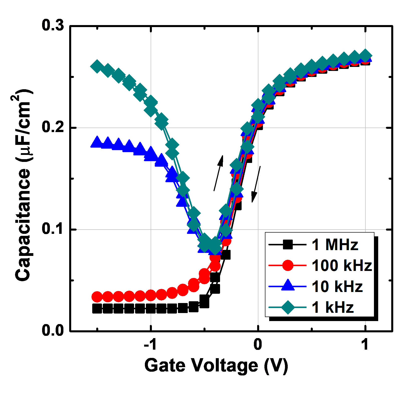
(a) Hysteresis of C-V characteristics as a function of air exposure time, where Ge/GeO2 stacks were exposed to air before the gate electrode formation. (b) Comparison of desorbed H2O in HPO-grown and APO-grown GeO2 films after 5-day air exposure. Thermal desorption spectroscopy is used to measured H2O molecules desorbing from GeO2 film. It shows that APO-grown GeO2 film has about 40% more H2O molecules than HPO-grown one, indicating that HPO-grown GeO2 film has a higher hygroscopic tolerance.
4.   Conclusion
The Ge thermal oxidation for the formation of high-quality Ge/GeO2 stack has been studied. It is found that the Ge/GeO2 interface can be improved by the post oxidation anneal at low temperatures that GeO desorption doesn’t occur. It is helpful to passivate the interface defects at the Ge/GeO2 interface generated by the conventional thermal oxidation. However, high-quality GeO2 bulk properties can only be achieved by high-pressure oxidation (HPO) that grows GeO2 at high temperatures with suppressing GeO desorption. This was achieved by taking care of thermodynamic and kinetic control of the Ge/GeO2 interface. The optimization of HPO and post oxidation annealing, which can further improve both GeO2 bulk and Ge/GeO2 interface properties, will be the most suitable for the formation of high-quality Ge/GeO2 stack.
Acknowledgments
The author would like to thank Prof. Akira Toriumi, Prof. Kita Koji, Prof. Kosuke Nagashio, and Dr. Tomonori Nishimura at the University of Tokyo for their continuous support and encouragement, which induced the main results reviewed in this paper.
[1] C. H. Lee, T. Nishimura, N. Saido, K. Nagashio, K. Kita, and A. Toriumi, “Record-high Electron Mobility in Ge n-MOSFETs Exceeding Si Universality”, IEDM Tech Dig. pp. 457 (2009).
[2] D. Kuzum, T. Krishnamohan, A. Nainani, Y. Sun, P. A. Pianetta, H. S-. P. Wong, and K. C. Saraswat, “Experimental Demonstration of High Mobility Ge NMOS”, IEDM Tech. Dig., pp. 453 (2009).
[3] K. Morii, T. Iwasaki, R. Nakane, M. Takenaka and S. Takagi, “High Performance GeO2/Ge nMOSFETs with Source/Drain Junctions Formed by Gas Phase Doping”, IEDM Tech. Dig., pp. 681 (2009).
[4] T. Nishimura, C. H. Lee, S.K. Wang, T. Tabata, K. Kita, K. Nagashio, and A. Toriumi, “Electron Mobility in High-k Ge MISFETs Goes up to Higher”, Symp. VLSI Tech. Dig., pp. 209 (2010).
[5] C. H. Lee, T. Nishimura, T. Tabata, S.K. Wang, K. Nagashio, K. Kita and A. Toriumi, “Ge MOSFETs Performance: Impact of Ge Interface Passivation”, IEDM Tech. Dig., pp. 416 (2010).
[6] R. Zhang, N. Taoka, P. Huang, M. Takenaka and S. Takagi, “1-nm-thick EOT High Mobility Ge n- and p-MOSFETs with Ultrathin GeOx/Ge MOS Interfaces Fabricated by Plasma Post Oxidation”, IEDM Tech. Dig., pp. 642 (2011).
[7] R. Zhang, P.-C. Huang, J.-C. Lin, M. Takenaka and S. Takagi, “Physical Mechanism Determining Ge p- and n-MOSFETs Mobility in High Ns Region and Mobility Improvement by Atomically Flat GeOx/Ge Interfaces”, IEDM Tech. Dig., pp. 371 (2012).
[8] C. H. Lee, C. Lu, T. Tabata, W. F. Zhang, T. Nishimura, K. Nagashio, and A. Toriumi, “Oxygen Potential Engineering of Interfacial Layer for Deep Sub-nm EOT High-k Gate Stacks on Ge”, IEDM Tech. Dig., pp. 40 (2013).
[9] K. Kita, C. H. Lee, T. Nishimura, K. Nagashio and A. Toriumi, “Control of Properties of GeO2 Films and Ge/GeO2 Interfaces by the Suppression of GeO Volatilization”, ECS Transaction, 19 (2), pp. 101 (2009).
[10] D. Kuzum, T. Krishnamohan, A. J. Pethe, A. K. Okyay, Y. Oshima, Y. Sun, J. P. McVittie, P. A. Pianetta, P. C. McIntyre, K. C. Saraswat, “Ge-Interface Engineering With Ozone Oxidation for Low Interface-State Density”, IEEE Elec. Dev. Lett., vol. 29, pp. 328 (2008).
[11] F. Bellenger, M. Houssa, A. Delabie, V. Afanasiev, T. Conard, M. Caymax, M. Meuris, K. De Meyer, and M. M. Heyns, “Passivation of Ge(100)/GeO2/high-k Gate Stacks Using Thermal Oxide Treatments”, J. Electrochem. Soc., vol. 155 (2), pp. G33 (2008).
[12] A. Delabie, A. Alian, F. Bellenger, M. Caymax, T. Conard, A. Franquet, S. Sioncke, S. Van Elshocht, M. M. Heyns, and M. Meuris, “H2O- and O3-based Atomic Layer Deposition of High-k Dielectric Films on GeO2 Passivation Layer”, J. Electrochem. Soc., vol. 156, pp. pp. G163 (2009).
[13] R. Zhang, T. Iwasaki, N. Taoka, M. Takenaka and S. Takagi, “Al2O3/GeOx/Ge Gate Stacks with Low Interface Trap Density Fabricated by Electron Cyclotron Resonance Plasma Post Oxidation”, Appl. Phys. Lett., vol. 98, pp. 112902 (2011).
[14] A. Wada, R. Zhang, S. Takagi, and S. Samukawa, “High-quality germanium dioxide thin films with low interface state density using a direct neutral beam oxidation process”, Appl. Phys. Lett., vol. 100, pp. 213108 (2012).
[15] R. Zhang, X. Tang, X. Yu and Y. Zhao, “Aggressive EOT scaling of Ge pMOSFETs with HfO2/AlOx/GeOx gate stacks fabricated by ozone post oxidation”, IEEE Elec. Dev. Lett., vol. 37, pp. 831 (2016).
[16] C. H. Lee, T. Tabata, T. Nishimura, K. Nagashio, K. Kita, and A. Toriumi, “Ge/GeO2 Interface Control with High-Pressure Oxidation for Improving Electrical Characteristics”, Appl. Phys. Exp., vol. 2, pp. 071404 (2009).
[17] K. Nagashio, C. H. Lee, T. Nishimura, K. Kita, and A. Toriumi, “Thermodynamics and kinetics for suppression of GeO desorption by high pressure oxidation of Ge”, Mater. Res. Soc. Symp. Proc., vol. 1155, pp. C06–02 (2009).
[18] M. Lenzlinger and E. H. Snow, “Fowler-Nordheim Tunneling into Thermally Grown SiO2”, J. Appl. Phys., vol. 40, pp. 278 (1969).
[19] S. Sasada, Y. Nakakita, M. Takenaka, and S. Takagi, “Surface orientation dependence of interface properties of GeO2/Ge metal-oxide-semiconductor structures fabricated by thermal oxidation”, J. Appl, Phys., vol. 106, pp. 073716 (2009).
[20] N. M. Ravindra, R. A. Weeks, and D. L. Kinser, “Optical properties of GeO2”, Phys. Rev. B, vol. 36, pp. 6132 (1987).
[21] T. Hosoi, K. Kutsuki, G. Okamoto, M. Saito, T. Shimura, and H. Watanabe, “Origin of flatband voltage shift and unusual minority carrier generation in thermally grown GeO2/Ge metal-oxide-semiconductor devices”, Appl. Phys. Lett., vol. 94, pp. 202112 (2009).
Article and author information
ChoongHyun Lee
chlee01@zju.edu.cn
Publication records
Published: June 29, 2020 (Versions1
References
Journal of Microelectronic Manufacturing