Research Article Archive Versions 1 Vol 3 (4) : 20030402 2020
Download
BSIM-CMG compact model for IC CAD: from FinFET to Gate-All-Around FET Technology
: 2020 - 10 - 02
: 2020 - 12 - 08
: 2020 - 12 - 30
1673 93 0
Abstract & Keywords
Abstract: We discuss the BSIM-CMG compact model for SPICE simulations of any common multi-gate (CMG) device. This is an industry standard model which has been used extensively for FinFETs IC design and simulation, and has now been extended to accurately model gate-all-around FET (GAAFET). We present the core framework of BSIM-CMG and discuss the latest updates that capture various physical phenomena originating from the quantum confinement of electrons by the small cross section of the GAAFET channel. Special attention is paid to providing suitable model parameters that can be adjusted using software tools to match the model with manufactured transistors very accurately. Furthermore, the model’s speed allows the use of Monte Carlo circuit simulation to account for random device variations encountered in manufacturing. This model is the industry standard compact model for GAAFETs and will help bridge the wide divide between GAA IC manufacturing and design, starting at 3nm/2nm technologies.
Keywords: gate-all-around; GAAFET; FinFET; BSIM; BSIM-CMG; compact model; quantum; nanosheet; 3D; transistor
1.   Introduction
Semiconductor devices have continuously improved over the past few decades in terms of density, performance and power consumption. This has been brought about mainly by scaling of transistors [1,2]. One of the most significant events for the semiconductor industry was the shift to FinFETs [1,2]. The design of these devices allows a gate on three sides of the channel resulting in greater gate control. This is of utmost importance to negate the side-effects of scaling (short channel effects). Moreover, the 3D vertical structure reduces the area requirement and allows further increase of the circuit density.
To continue scaling further, we require even greater gate control. The next logical step after FinFETs is to have gate on all sides of the channel; giving rise to the Gate-All-Around FET (GAAFET), as shown in Figure 1 [3-6]. Several companies have recently announced the use of GAAFETs for production design [3-10]. This device not only provides excellent gate control, but also utilizes a vertical structure with multiple channels per fin to reduce the footprint even further [7].
Designing circuits with such devices requires a compact model for SPICE simulators. The device model is a set of equations that describe the device behavior and can be evaluated very fast so that very large circuits can be simulated while being able to reproduce the very complex transistor characteristics accurately. It needs to be accurate to avoid expensive re-designs, very fast to enable timely simulation of large circuits as well as robust to ensure convergence for a wide range of complex circuits and simulation conditions [2]. BSIM-CMG is the industry standard models for common-multi-gate (CMG) devices like FinFETs and GAAFETs. The model can accurately simulate double gate, triple gate, quadruple gate and gate-all-around structures of any geometry including commercial FinFET and GAAFET devices.
In this paper, we will provide an overview of the BSIM-CMG compact model with special emphasis on GAAFETs.


Figure 1.   (a) Graphical representation of FinFET and GAAFET. The GAAFET structure. (b) GAAFET cross-section used for band-structure TCAD simulations; illustrating the width (WSi), thickness (TSi) and the corner radius (rc).
2.   BSIM-CMG Core Framework
The BSIM-CMG model is a compact (SPICE) model for common-multi-gate devices [2]. It is based on a core modelwhich calculates the device electrostatics and transport using a long-channel assumption. Physical effects like short channel effects, leakage currents, non-quasi-static effects, noise etc., are added on top of the core model as demonstrated in Figure 2.
The core electrostatics is based on the Poisson equation with several approximations. The core equation can be given as [2,15]
(1)
where v0 and qt represent
(2)
(3)
In these equations, q is the electronic charge, ni is the intrinsic carrier concentration, vT is the thermal voltage, is the normalized gate voltage, and is the normalized channel voltage. Also, with Qm denoting the mobile charge density and is the normalized depletion charge density. The term rN is defined as ,where ϵch is the permittivity of the channel and AFin is the area of the fin. The term Δqdep accounts for the effect of body bias for FinFETs fabricated over bulk substrates. This term is defined as [15]
(4)
where is the body-effect parameter and ni is the intrinsic carrier concentration.


Figure 2.   An illustration of the BSIM-CMG compact model framework.
This model is valid for any cross-section shape and depends only on four terms: (i) Ach , denoting the area of cross-section the channel i.e. the area of the blue region in Figure 1(b), (ii) Weff , denoting the effective width of the channel for carrier transport, i.e., the perimeter of the blue region in Figure 1(b), (iii) Nch , representing the doping in the channel, and (iv) Cins , representing the insulator capacitance per unit length, i.e. the capacitance of the yellow region in Figure 1(b), assuming the length (into the paper) is unity. Table 1 provides some examples of calculating these four terms.
Table 1.   Model parameter examples. R denotes the radius of cylindrical nanowire. HFin and TFin are the height and thickness of fin, and rc is the radius of curvature of corners in GAAFETs.
Double-gateTri-gateCylindrical nanowireGAAFET/Nanosheet
Weff
Ach
Cins
NchChannel dopingChannel dopingChannel dopingChannel doping
In Equation (1), the three terms on the right hand side define the behavior of the charge density in the channel. The linear term dominates in strong inversion, the second term dictates weak-inversion and the third is for the moderate inversion region. This equation, therefore, models the behavior of the channel charge accurately for all bias regions [15]. The core transport equation is the well-known drift-diffusion model [2], given as
(5)
where . Also qm,S and qm,D are the normalized mobile charge densities at the source and the drain ends, respectively. Second order effects (like various short channel effects) are added on top of Equation (5) [2]. For GAAFET devices with multiple channels per fin, the model scales the calculated quantities appropriately to get the correct terminal characteristics.
3.   GAAFET Module
The BSIM-CMG framework has the ability to simulate GAAFETs [2,15]. Recently, however, a few important new code modules have been added to capture the GAAFET specific effects like geometry dependent quantum effects and mobility degradation [13,14]. A new parasitic capacitance network has also been added to capture the effects of the GAAFET structure. In the following subsections we will discuss the most significant GAAFET specific physics that affect the core model behavior.
3.1.   Electrostatics
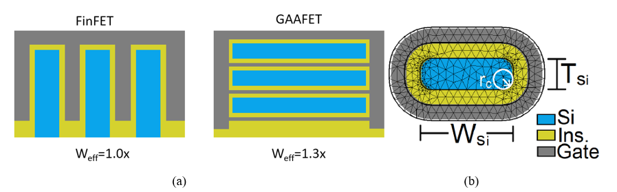
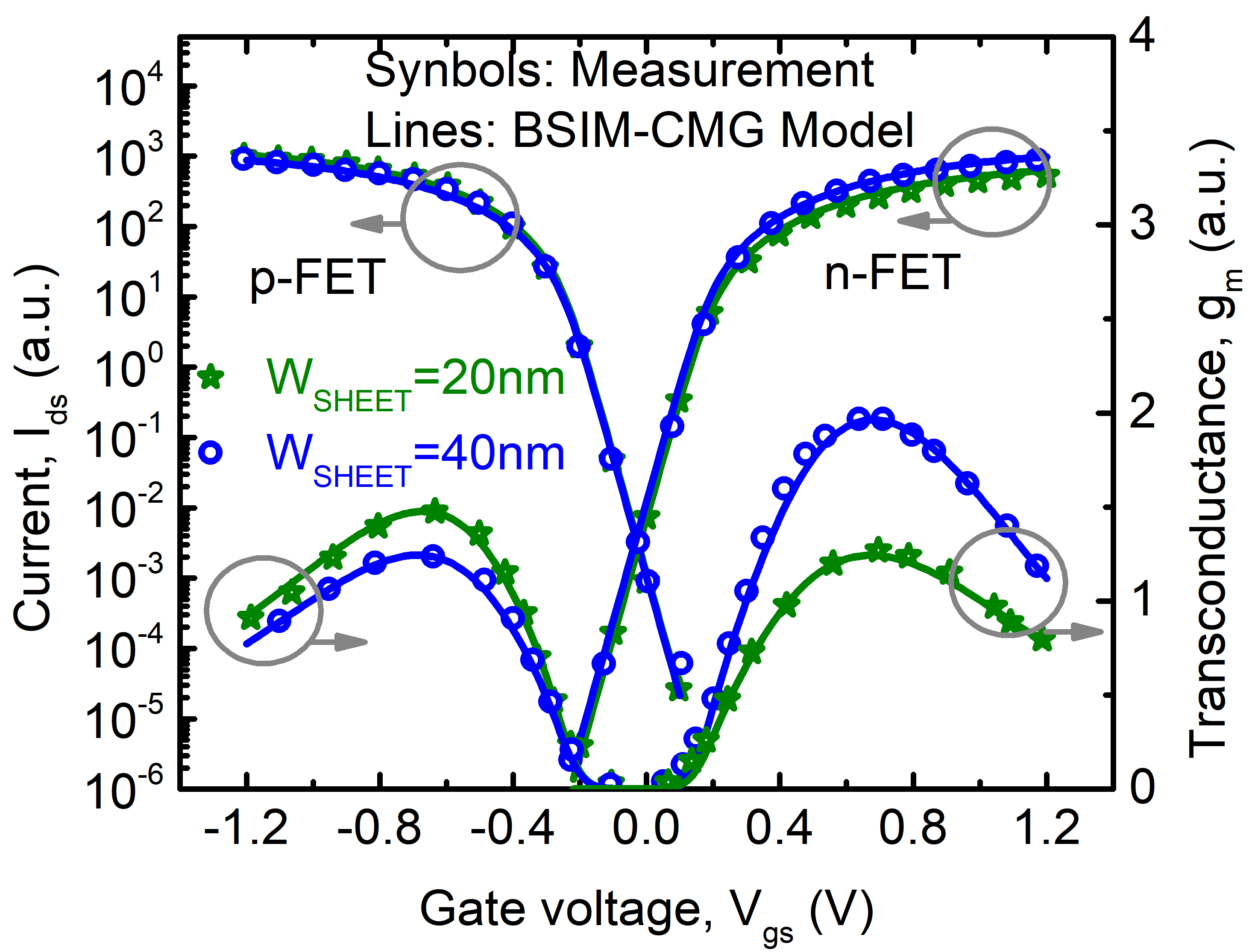
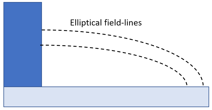
BSIM-CMG, through a geometry module (GEOMOD=5), can calculate accurate values of Ach , Cins and Weff ; which are then used in the core model to get the electrostatic behavior, as described in Section 2. The calculation of Ach and Weff include the effects of rounded corners (Figure 1). This model also has the ability to accurately simulate multiple GAA bodies in a single fin (stack). The user can specify various geometry details like the width and thickness of the GAA bodies, the separation between GAA bodies, the number of GAA bodies per fin, fin height etc. The model takes all this geometry information to calculate the electrostatics accordingly. The model can also account for geometry variation among the GAA bodies inside a single fin. In addition to accounting the aforementioned geometry variations, the model further supports Monte Carlo circuit simulation to account for the stochastic device geometric variations that may be encountered in manufacturing.
A significant impact of the confined channel of GAAFETs is the quantum confinement effect on the density of states of silicon. This affects the bias dependence of the channel mobile charge; which in turn affects all device characteristics. To understand the various quantum mechanical effects that play a role, consider the charge in a semiconductor, which can be written as
(6)
where is the density of states for the ith subband, Ef is the fermi energy and Fj () is the Fermi integral of order j. The term, , is given as
(7)
where Di is the electrostatic dimension for the ith subband, is the effective mass of the ith subband and is the Planck’s constant. In BSIM-CMG, the user is allowed to choose up to 3 subbands and can modify individual subband parameters (refer Table 2).


Figure 3.   
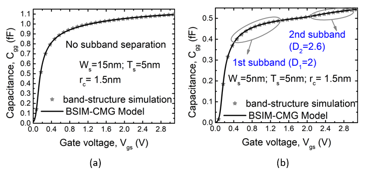
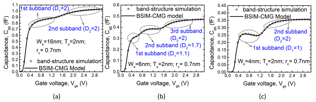
The plots show the gate capacitance with varying gate voltage; for channel thickness of 5nm. For larger cross-sections, like in (a), the confinement is non-existent. Extreme width confinement, as shown in (b), results in a small effect of subband separation.


Figure 4.   
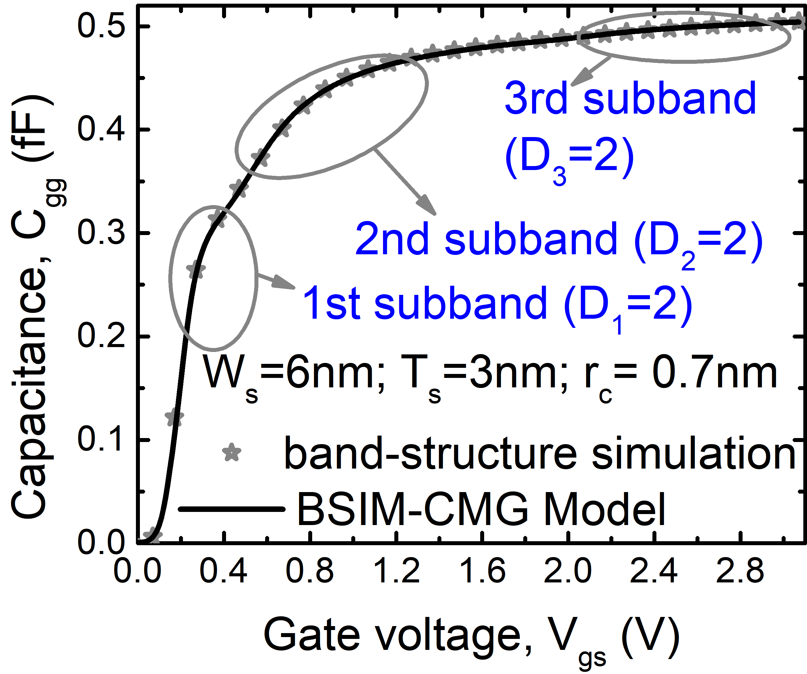
The plot shows the gate capacitance with varying gate voltage; for channel thickness of 3nm. For confined widths, the subband effects are quite pronounced and the overall electrostatic dimension reduces to 2D.
With changing cross-section, the electrostatic dimension Di changes. It was recently pointed out that while 1D and 2D are popular and important special cases of quantum confined state, the electrostatic dimension can be a continuous variable. BSIM-CMG is the first compact model that accounts for this fact and can therefore accurately model GAAFET for continuously variable width, WSi [13] . For very confined channels, the system generally has lower dimension. For example, thin and wide channels behave as 2D systems whereas thin and narrow channels are confined in the width direction also, resulting in a 1D behavior. With decreasing confinement, the dimension gradually changes to higher values (2D/3D). This behavior is shown in Figure 3, Figure 4, and Figure 5, where the plots show capacitances (which mimic the density of states) for various cross-sections. As confinement reduces, the dimension shifts from lower to higher values.
Figure 4 and Figure 5 also shows peaks and valleys in the capacitance. These occur due to subband separation. For very confined devices, the conduction band splits up into subbands resulting in peaks in the density of states; which are reflected in the capacitance plots. With increasing confinement, the subband energies increase and they move further apart as illustrated in Figure 5. For larger cross-sections the subband energies reduce and they come closer in energy; forming continuous conduction band. The subband model has been discussed in detail in [13].


Figure 5.   
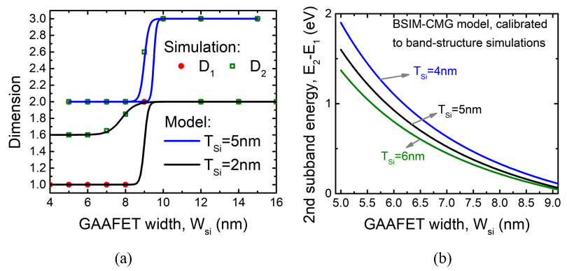
The plots show the gate capacitance with varying gate voltage; for different GAAFET thickness=2nm. The confinement changes from 2D to 1D with decreasing GAAFET width.
Figure 6 (a) shows the variation of the electrostatic dimension with changing GAAFET width for 2nm thick channels (black line). As confinement reduces with increasing width, the dimension changes from 1D to 2D. The maximum dimension is restricted by the thickness confinement (2nm) and is hence limited to 2D. For thicker GAAFET devices (5nm) the maximum dimension goes up to 3D, as shown by the blue lines. Figure 6 (b) shows the variation of the second subband energy for different cross-sections.
The capacitance (or charge) also depends on the effective mass, as shown in Equation (6) and Equation (7). The effective mass changes with confinement, and so does the bandgap. The effective mass contributes not only to the charge but also affects mobility. However, the effective mass formulations used in the electrostatics and transport are different. For both these effective mass calculations, we have parameters to modify the geometry dependence based on the device type, material, etc. The geometry dependence of the effective mass for the i-th subband in electrostatics calculations is given as
(8)
where , γ0, αm , βm and κm are device dependent parameters. can be used as a fitting parameter to tune the variation of effective mass for each subband. Note that the variation of effective mass in Silicon is quite complex since longitudinal and transverse masses react differently to confinement. However, for compact modeling purposes, we use have developed a single expression for geometry dependence of effective mass for electrostatics which has been described in Equation (8) [13].
The bandgap on the other hand plays a role in deciding the threshold voltage. With increasing confinement, both the bandgap and the effective mass increase. This increases the threshold voltage and reduces the amount of charge at a given voltage; as can be seen in Figure 5, Figure 4, and Figure 3.


Figure 6.   
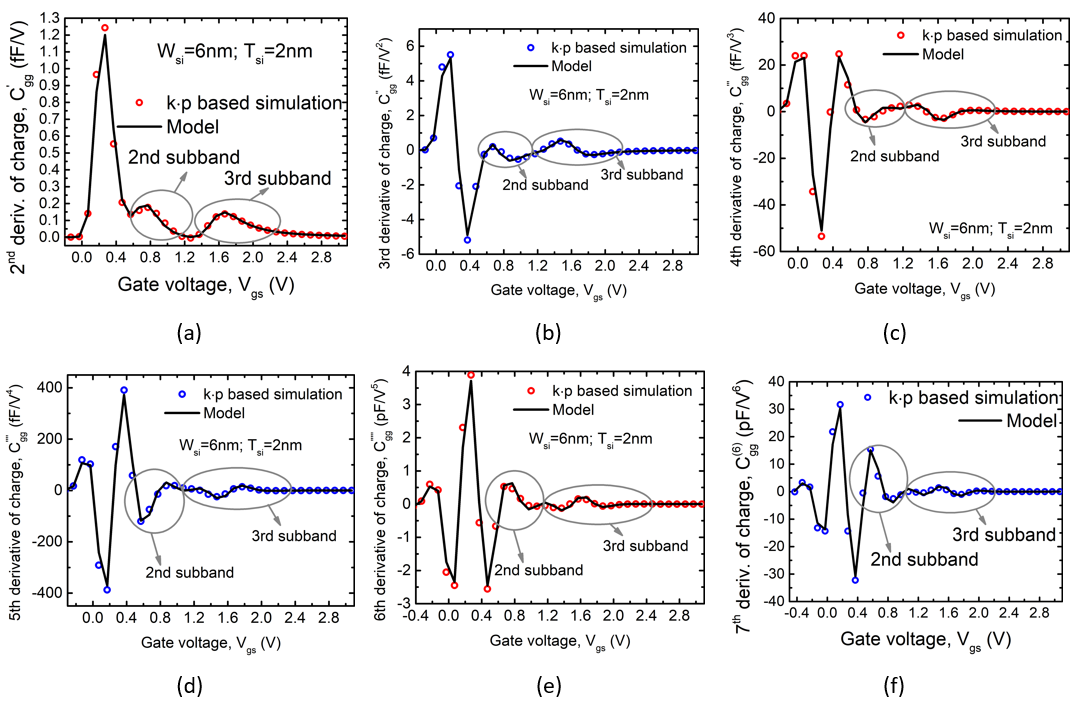
(a) Variation of dimensions for the first and second subbands with thicknesses of 2nm (black lines) and 5nm (blue lines). (b) Variation of the second subband energy, with respect to the first subband energy, for various GAAFET widths and thicknesses.
Another key requirement from the compact model is accuracy for derivatives of charges and currents. The peaks and valleys due to quantum confinement lead to multiple secondary peaks in the derivatives of charges. It is important that the compact model captures this to ensure high accuracy for analog/RF simulations. We have developed and tested our model up to the seventh derivative of charge to ensure high accuracy in non-linearity and harmonics simulations. Figure 7 shows the model results for multiple orders of derivatives along with the simulation results to validate this.
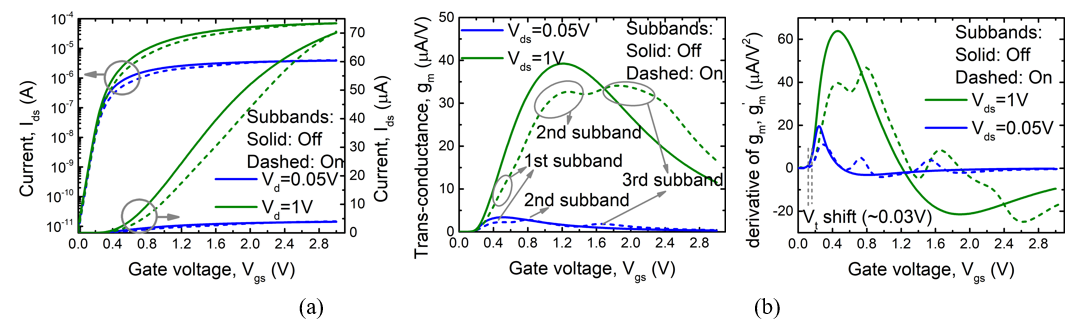
The impact of confinement can also be seen in terminal currents. Figure 8 shows the drain-to-source current along with the transconductance and the derivative of the transconductance for WSi =6nm and TSi =2nm. The simulation has been done with a constant mobility to remove the effects of confinement on mobility. Impact of electrostatic confinement can be clearly seen in plots. Not only does the current reduce due to lower density of states, the effect of subband separation is also seen as distinct peaks and valleys in the derivatives.


Figure 7: Derivates of charge from 1st to 7th order showing the accuracy of the model for higher order derivatives.


Figure 8.   Variation of (a) drain current, (b) transconductance and (c) derivative of transconductance with gate voltage. The solid and dashed lines are the simulation results with and without quantum confinement effects.
3.2.   Transport
In the BSIM-CMG framework, all the transport physics is captured through the concept of effective mobility(μ)[14]. The field dependence of mobility is captured through
(9)
where is the effective mobility at low transverse electric field, α and β are parameters and Eeff is the effective transverse electric field. For GAAFETs (as well as FinFETs) the effective mobility is dependent on the Silicon thickness, as shown in Figure 9. Note that the mobility, in general, reduces with increasing confinement. There are multiple factors that contribute to the geometry dependence of mobility, which have been captured through the concept of effective mass. From Figure 9, we can see that high confinement results in the reduction of the effective mobility (μ) which can be modeled by an increasing effective mass. This can be captured through the following equation [14]
(10)
where and . Here m0 is the rest mass of an electron, μ0 is a parameter representing the mobility with effective mass = m0 . where h is the Planck constant and a0 is the lattice constant. Also, Eg,bulk is the band-gap for bulk Silicon and . Sm is a scaling factor used to tune the dependence for different materials, device types and dopings.


Figure 9.   Variation of mobility with inversion carrier density for different GAAFET thicknesses. The measurements are for a p-type device [9]. Mobility reduces with reduction in thickness because of the increase in effective mass with increasing confinement. Moreover, the field dependence of the mobility also changes with reduction of the thickness.
The change in effective mass is not enough to capture the geometry dependence of mobility. It is important to note that the field dependence of mobility (high inversion charge) also changes with increasing confinement. This region is dominated by phonon-scattering and surface roughness scattering. This has been captured by including geometry dependence in α and β terms of Equation (9) [14].
Another phenomenon of geometry dependent mobility variation specific to GAAFETs is the effect of the different crystal orientations of the top/bottom surface and the sidewalls. Since these two surfaces are oriented differently, the mobilities for the sidewall and the top/bottom surfaces are different. This leads to the mobility depending on the width as well as thickness of the GAA body and the scaling being a function of the width and thickness. Moreover, the ratio of the mobility of the sidewall to that of the top/bottom surface () may be less than unity for electrons and more than unity for holes; leading to completely opposite scaling trends for n-type and p-type devices, as shown in Figure 10. This effect has also been captured in the latest BSIM-CMG GAAFET model [14] as
(11)


Figure 10.   Effect of different mobilities at the sidewall and the top/bottom surface. The mobility scales differently with width scaling for n-type and p-type devices since the ratio of mobilities at the sidewall and top/bottom surface are different for electrons and holes.
The final expression for mobility is given as [14]
(12)
4.   Parasitic Capacitance
BSIM-CMG includes models for calculation of parasitic capacitances for various device geometries. Accurate modeling of parasitic capacitances plays a crucial role in the accurate analog, digital and RF simulations. Since there are differences between the device structures of FinFETs and GAAFETs, as shown in Figure 1, the latest BSIM-CMG model also has a specific module (CGEOMOD=3) for accurate parasitic capacitance calculation for GAAFET devices. This module takes into account the various structural details of the fin as well as the GAA channels inside it to calculate the various parasitic capacitance elements. The model has the ability to account for multiple GAA channels per fin as well as the parasitic FinFET, indicated in Figure 11(b) which shows the various components of parasitic capacitance for FinFETs and GAAFETs. The GAAFET structure has a more complex parasitic capacitance network because of the multiple GAA channels per fin.


Figure 11.   Graphical representation of the parasitic capacitance components for FinFETs and GAAFETs. As can be seen, the GAAFET structure has additional components due to the multiple channels per fin.
Some of the fringe capacitance components are explicitly shown in Figure 11(c). Due to the curved 3D structure of FinFET and GAAFET channels, the corner components are different from the central ones. Moreover, the GAAFET structure has total six components of fringe capacitance per channel as opposed to only three components for the fin in case of FinFETs. For example, Cd has three components: one for the central region and two for the two corners, as shown in Figure 11(b). This is also true for Ce, Cf, Cg etc. The model for fringe capacitances is derived by summing over the capacitances of small area elements as
(13)
where ΔC is the capacitance corresponding to the infinitesimal area element ΔA, ϵ is the effective permittivity of the insulating material and d is the effective thickness of the insulator. Note that the structure of these devices often does not result in simple parallel-plate capacitance scenarios with straight field-lines. In most cases, the two surfaces of the capacitor are at some angle (mostly orthogonal) to each other and the field-lines curve from one surface to the other. In such cases, the effective d is calculated using the length of the field-line assuming that the field-lines follow an ellipse, as shown in Figure 12 [2]. For orthogonal surfaces, the effective distance is a quarter of the perimeter of an ellipse given by
(14)
where a and b are the length of the major and minor axes of the ellipse, respectively.
The calculation of overlap capacitances also changes from FinFET to GAAFET since the overlap length changes because of the GAAFET structure. Also, multiple GAAFET channels in a single fin requires the overlap capacitance of a single GAAFET be scaled by the total number of channels per fin to ensure that the terminal characteristics are captured correctly [2].


Figure 12.   Graphical representation capacitance calculation for orthogonal surfaces.
5.   Model Parameters
BSIM-CMG provides the model user with carefully implemented model parameters that can be adjusted using software tools to match the model to manufactured transistors very accurately. This crucial step is performed by the foundry of the fab of an integrated device manufacturer. One may say that a device model is the model code, such as BSIM-CMG, plus a specific parameter value set. For example, the difference between Samsung 3nm GAA transistors and TSMC 2nm GAA transistors are captured and represented by two difference sets of the BSIM-CMG parameters. These parameters, about forty in number for the GAA related effects, in conjunction with the device information that the IC designer specifies, such as the width of the GAA channel and the length of the GAA gate, are used by computer-aided IC design tools to simulate, design and optimize circuits. Some of the key parameters for GAAFET devices are specified in Table 2.
Simulation speed is also a key characteristic of a good compact models. BSIM-CMG includes all of necessary physics while rapidly calculating all the terminal currents and charge (for capacitive currents) for any given terminal voltages. The speed allows the use of Monte Carlo circuit simulation to account for random device variations encountered in manufacturing. The compact model also provides some parameters to allow the model user to optimize their simulation accuracy versus time to best suit their requirements.
Table 2.   Selected BSIM-CMG parameters used in GAAFET modeling.
ParametersDescription
FPITCHFin pitch
TMASKHeight of the hard mask on top of the fin
TGATEGate height on top of hard mask
HEPIHeight of the raised source/drain on top of the fin
TSILIThickness of the silicide on top of the raised source/drain
WGAAWidth of GAA channel (represented by WSi in Figure 1b)
TGAAThickness of GAA channel (represented by TSi in Figure 1b)
DWS1/DWS2/DWS3Rounded corner correction for total channel perimeter of the 1st/2nd/3rd/ GAAFET; in case there are multiple GAAFETs per fin
DACH1/DACH2/DACH3Rounded corner correction for total channel area of the 1st/2nd/3rd/ GAAFET; in case there are multiple GAAFETs per fin
TSUSDistance between multiple GAAFETs per fin
NGAANumber of GAA per fin
HPFFHeight of parasitic FinFET
U0ETAWSCRatio of the mobility of the sidewall to that of the top/bottom surface
EGBULKBulk band-gap
6.   Conclusion
We have presented the BSIM-CMG compact model framework; with emphasis on the modeling of GAAFETs. This compact model has been extensively used by the semiconductor industry for FinFET based IC designs. We have discussed the model core which forms the backbone for all the calculation. We have also discussed the latest modules that capture the potentially strong effects of quantum confinement on silicon density of states and transport in GAAFET devices. This model is the industry standard compact model for simulating and designing GAA ICs, libraries and IPs.
Acknowledgments
[1] X. Huang, W-C. Lee, C. Kuo, D. Hisamoto, L. Chang, J. Kedzierski, E. Anderson, H. Takeuchi, Y-K. Choi, K. Asano, V. Subramanian, T-J. King, J. Bokor, C. Hu, “Sub 50-nm FinFET: PMOS,” IEDM Technical Digest, Washington, DC, pp. 67-70, December 5-8, 1999.
[2] Y. S. Chauhan et al., “FinFET Modeling for IC Simulation and Design: Using the BSIM-CMG Standard”. New York, NY, USA: Academic, 2015, doi: 10.1016/B978-0-12-420031-9.09994-2.
[3] H. Mertens et al., “Vertically stacked gate-all-around Si nanowire CMOS transistors with dual work function metal gates,” in IEDM Tech. Dig., Dec. 2016, pp. 19.7.1–19.7.4, doi: 10.1109/IEDM.2016.7838456.
[4] M. Karner et al., “Vertically stacked nanowire MOSFETs for sub-10 nm nodes: Advanced topography, device, variability, and reliability simulations,” in IEDM Tech. Dig., Dec. 2016, pp. 30.7.1–30.7.4, doi: 10.1109/IEDM.2016.7838516.
[5] Y. Jiang et al., “Performance breakthrough in 8 nm gate length Gate-AllAround nanowire transistors using metallic nanowire contacts,” in Proc. Symp. VLSI Technol., Jun. 2008, pp. 34–38, doi: 10.1109/VLSIT.2008.4588553.
[6] Y. Cui et.al., “High performance silicon nanowire field effect transistors,” Nano Lett., vol. 3, no. 2, p. 149–152, 2003, doi: 10.1021/nl025875l.
[7] N. Loubet et al., “Stacked nanosheet gate-all-around transistor to enable scaling beyond FinFET,” in Proc. Symp. VLSI Technol., Jun. 2017, pp. T230–T231, doi: 10.23919/VLSIT.2017.7998183.
[8] K. H. Yeo et al., “Gate-all-around (GAA) twin silicon nanowire MOSFET (TSNWFET) with 15 nm length gate and 4 nm radius nanowires,” in IEDM Tech. Dig., Dec. 2006, pp. 1–4, doi: 10.1109/IEDM.2006.346838.
[9] C. W. Yeung et al., “Channel geometry impact and narrow sheet effect of stacked nanosheet,” in IEDM Tech. Dig., Dec. 2018, pp. 28.6.1–28.6.4, doi: 10.1109/IEDM.2018.8614608.
[10] G. Bae et al., “3 nm GAA technology featuring multi-bridge-channel FET for low power and high performance applications,” in IEDM Tech. Dig., 2018, pp. 28.7.1–28.7.4, doi: 10.1109/IEDM.2018.8614629.
[11] A. Dasgupta, A. Agarwal, and Y. S. Chauhan, “Unified compact model for nanowire transistors including quantum effects and quasi-ballistic transport,” IEEE Trans. Electron Devices, vol. 64, no. 4, pp. 1837–1845, Apr. 2017, doi: 10.1109/TED.2017.2672207.
[12] A. Dasgupta et.al., “Compact modeling of cross-sectional scaling in gate-all-around FETs: 3-D to 1-D transition,” IEEE Trans. Electron Devices, vol. 65, no. 3, pp. 1094–1100, Mar. 2018, doi: 10.1109/TED.2018.2797687.
[13] A. Dasgupta et.al., "BSIM Compact Model for Quantum Confinement in Advanced Nanosheet FETs", IEEE Transactions on Electron Devices, vol. 67, no. 2, 2020.
[14] A. Dasgupta et.al., "Compact Model for Geometry Dependent Mobility in Nanosheet FETs", IEEE Electron Device Letters, vol. 41, no. 3, 2020.
[15] J. P. Duarte et.al., “BSIM-CMG: Standard FinFET Compact Model for Advanced Circuit Design”, IEEE European Solid-State Circuit Conference (ESSCIRC), Graz, Austria, Sept. 2015.
[16] J. Wang et.al., “Bandstructure and orientation effects in ballistic Si and Ge nanowire FETs,” in IEDM Tech. Dig., Dec. 2005, p. 533, doi: 10.1109/IEDM.2005.1609399.
[17] Y. S. Chauhan et al., FinFET Modeling for IC Simulation and Design: Using the BSIM-CMG Standard. New York, NY, USA: Academic, 2015, doi: 10.1016/B978-0-12-420031-9.09994-2.
[18] B. Sorée, W. Magnus, and G. Pourtois, “Analytical and self-consistent quantum mechanical model for a surrounding gate MOS nanowire operated in JFET mode,” J. Comput. Electron., vol. 7, no. 3, pp. 380–383, 2008, doi: 10.1007/s10825-008-0217-3.
[19] S. Venugopalan et.al., “Phenomenological compact model for QM charge centroid in multigate FETs,” IEEE Trans. Electron Devices, vol. 60, no. 4, pp. 1480–1484, Apr. 2013, doi: 10.1109/TED.2013.2245419.
Article and author information
Avirup Dasgupta
avirup@berkeley.edu
Avirup Dasgupta is a postdoctoral scholar at the Department of Electrical Engineering and Computer Science, University of California, Berkeley, CA, USA. He is the manager of the Berkeley Device Modeling Center and a developer in the BSIM group.
Chenming Hu
hu@eecs.berkeley.edu
Chenming Hu is currently a Distinguished Professor Emeritus with the University of California at Berkeley, Berkeley, CA, USA. He is also a Board Director of SanDisk Inc., Milpitas, CA, USA, and the Friends of Children with Special Needs, Fremont, CA, USA
Publication records
Published: Dec. 30, 2020 (Versions1
References
Journal of Microelectronic Manufacturing