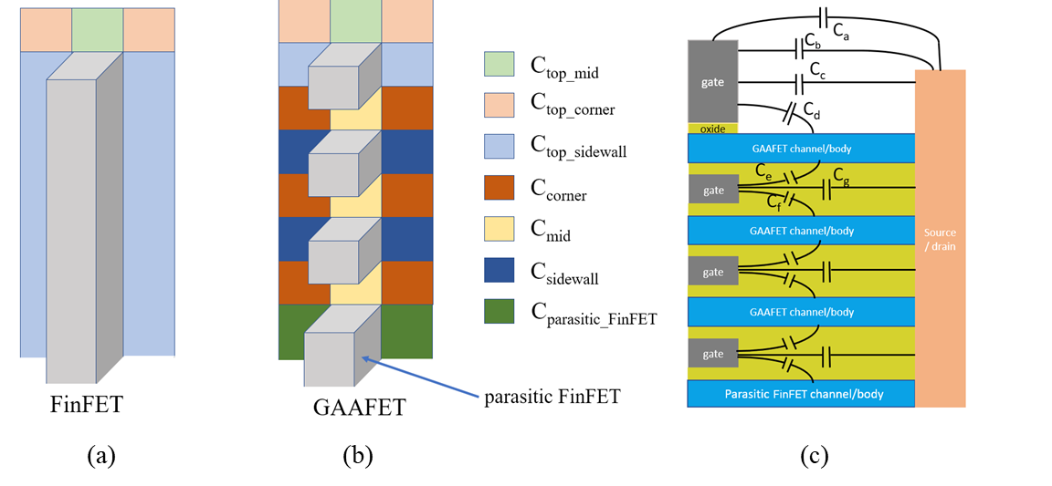
Authors: Avirup Dasgupta, Chenming Hu
Institution:Department of Electrical Engineering and Computer Science, University of California
Keywords:gate-all-around;GAAFET;FinFET;BSIM;BSIM-CMG;compact model;quantum;nanosheet;3D;transistor
doi:10.33079/jomm.20030402
Abstract:
We discuss the BSIM-CMG compact model for SPICE simulations of any common multi-gate (CMG) device. This is an industry standard model which has been used extensively for FinFETs IC design and simul...
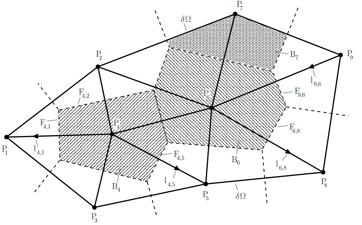
Authors: Bernd Meinerzhagen
Institution:Technical University Braunschweig
doi:10.33079/jomm.20030403
Abstract:
In 1964 Hermann Gummel published the first numerical solution method for the one-dimensional Drift Diffusion model. In his seminal paper [1] already the nonlinear iteration method and th...
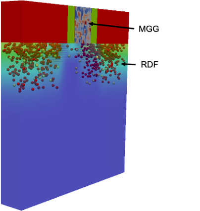
Authors: Cristina Medina-Bailon, Tapas Dutta, Fikru Adamu-Lema et al.
Institution:Device Modelling Group, James Watt School of Engineering, University of Glasgow
Keywords:Integrated Simulation Environment;Variability;Drift-Diffusion;Quantum Correction;Kubo-Greenwood;Non-Equilibrium Green’s Function
doi:10.33079/jomm.20030404
Abstract:
This paper presents the latest status of the open source advanced TCAD simulator called Nano-Electronic Simulation Software (NESS) which is currently under development at the Device Modeling Group ...
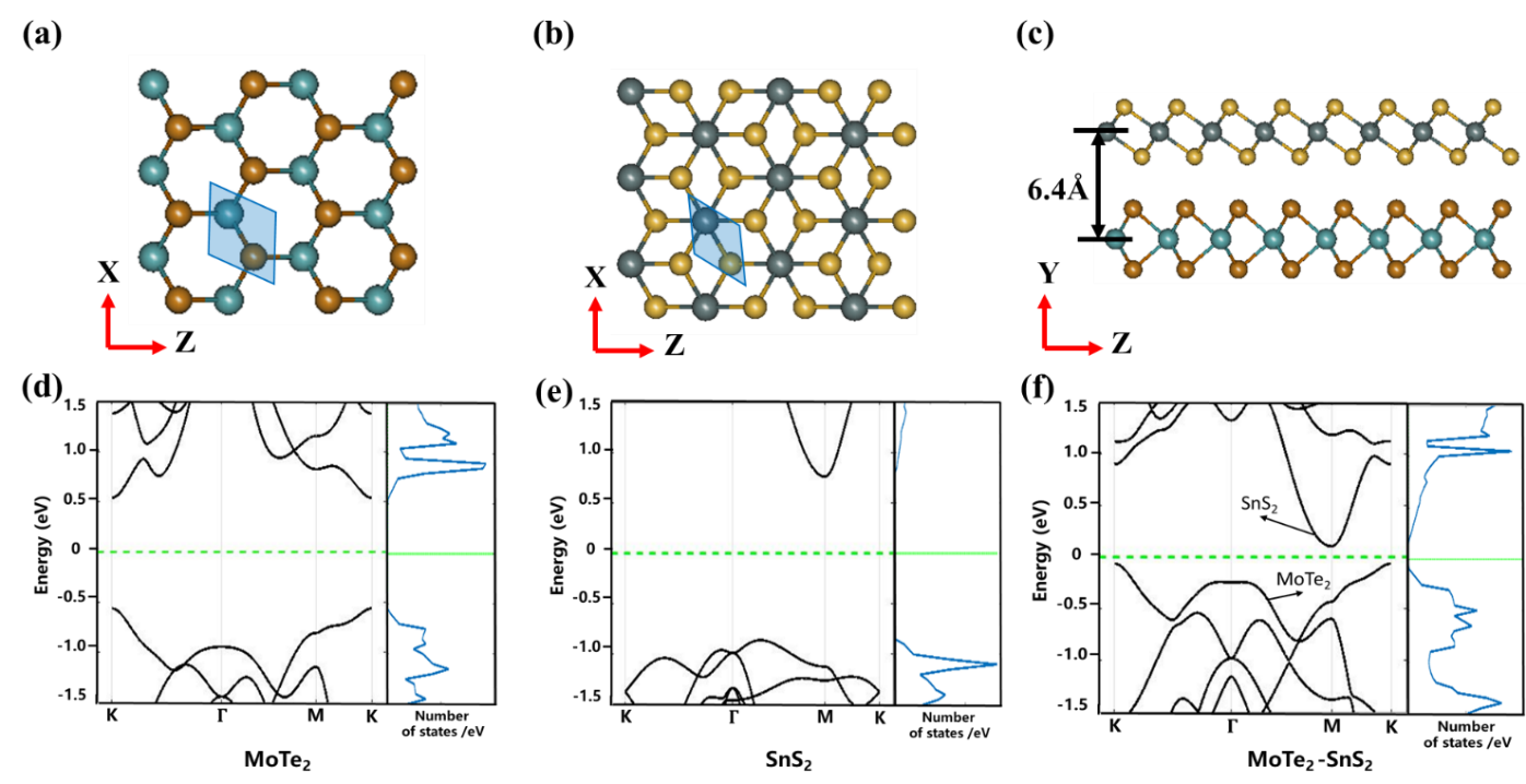
Authors: Kun Luo, Kui Gong, Jiangchai Chen et al.
Institution:Key Laboratory of Microelectronics Device and Integrated Technology, Institute of Microelectronics of Chinese Academy of Sciences
Keywords:2D materials heterojunction;tunnel-FET;gate-to-drain overlap;DFT-NEGF
doi:10.33079/jomm.20030405
Abstract:
The electronic properties and transport properties of MoTe2/SnS2 heterostructure Tunneling FETs are investigated by the density functional theory coupled with non-equilibrium ...
Authors: Boris A. Voinov, Patrick H. Keys, Stephen M. Cea et al.
Institution:Logic Technology Development, Intel Corporation, Hillsboro OR
Keywords:TCAD;atomistic modeling;density functional theory;molecular dynamics;kinetic Monte Carlo
doi:10.33079/jomm.20030406
Abstract:
During the past decade, significant progress has been achieved in the application of material modeling to aid technology development in semiconductor manufacturing companies such as Intel. In this ...
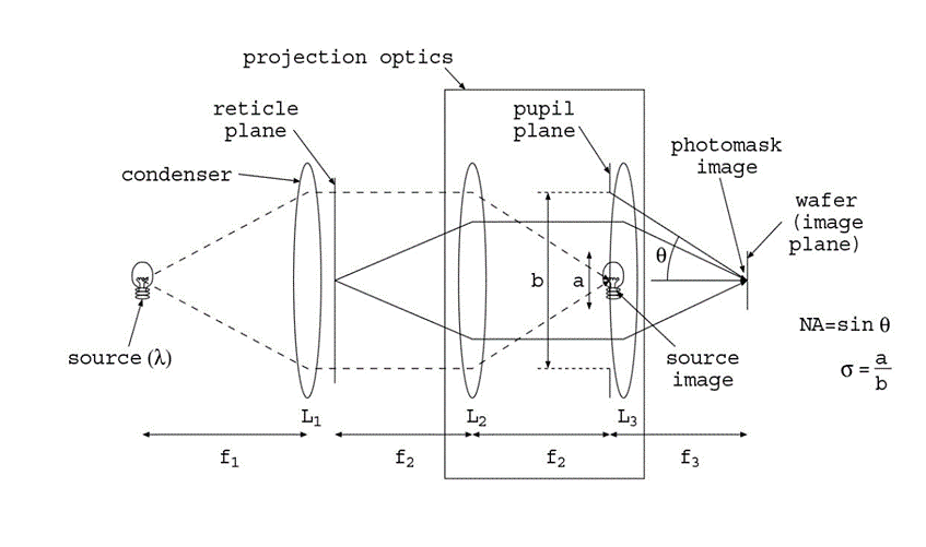
Authors: Xuelong Shi, Yan Yan, Tao Zhou et al.
Institution:Shanghai IC Research and Development Center, Shanghai
Keywords:Optimal feature maps;inverse lithography technology (ILT);deep convolution neural network (DCNN)
doi:10.33079/jomm.20030407
Abstract:
Inverse lithography technology (ILT) is intended to achieve optimal mask design to print a lithography target for a given lithography process. Full chip implementation of rigorous inverse lithograp...
Authors: Pengpeng Yuan, Taian Fan, Yaobin Feng et al.
Institution:Institute of Microelectronics, Chinese Academy of Science, Beijing
Keywords:optical proximity correction;machine learning;deep learning;lithography
doi:10.33079/jomm.20030408
Abstract:
The shrinking of the size of the advanced technological nodes brings up new challenges to the semiconductor manufacturing community. The optical proximity correction (OPC) is invented to reduce the...
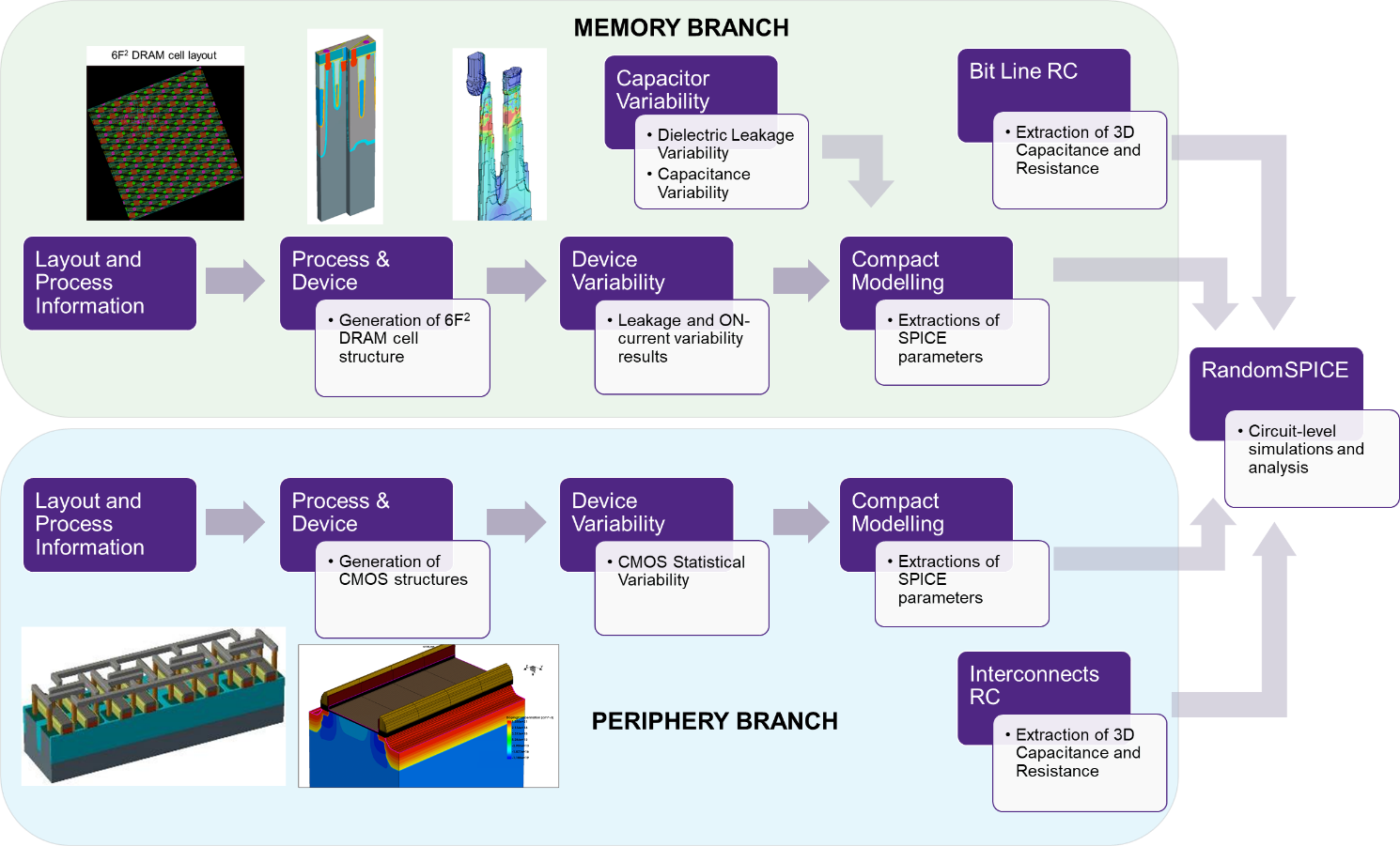
Authors: Salvatore M. Amoroso, Plamen Asenov, Jaehyun Lee et al.
Institution:Synopsys Europe, Ltd.
Keywords:DTCO;Statistical Variability;Process Variability;Semiconductor Memories;DRAM;CMOS;Scaling
doi:10.33079/jomm.20030409
Abstract:
This paper presents a TCAD-based methodology to enable Design-Technology Co-Optimization (DTCO) of advanced semiconductor memories. After reviewing the DTCO approach to semiconductor devices scalin...
Authors: Chenmin Hu, Khurram Zafar, Abhishek Vikram et al.
Institution:Anchor Semiconductor, Santa Clara
Keywords:Die-to-Database;Full Chip Decomposition;Machine Learning;Defect Discovery;Pattern Fidelity;Pattern Risk Scoring;OPC Verification;Process Window Qualification
doi:10.33079/jomm.20030410
Abstract:
Chip designers employ computer-aided design, circuit simulation, and design rule check systems. Lithography engineers employ model-based OPC (Optical Proximity Correction) and model-based print-sim...