Research Article Current Issue Versions 2 Vol 3 (4) : 20030409 2020
Download
Enabling Variability-Aware Design-Technology Co-Optimization for Advanced Memory Technologies
: 2020 - 09 - 29
: 2020 - 12 - 22
: 2020 - 12 - 30
1859 67 0
Abstract & Keywords
Abstract: This paper presents a TCAD-based methodology to enable Design-Technology Co-Optimization (DTCO) of advanced semiconductor memories. After reviewing the DTCO approach to semiconductor devices scaling, we introduce a multi-stage simulation flow to study the device-to-circuit performance of advanced memory technologies in presence of statistical and process variability. We present a DRAM example to highlight the DTCO enablement for both memory and periphery. Our analysis demonstrates how the evaluation of different possible technology improvements and design combinations can be carried out to maximize the benefits of continuous technology scaling for a given set of manufacturing equipment.
Keywords: DTCO; Statistical Variability; Process Variability; Semiconductor Memories; DRAM; CMOS; Scaling
1.   Introduction
The pace of the technology roadmap for semiconductor was conventionally marked by scaling of the patterning pitches, with the main goal to halve the cost per transistor at each subsequent technology node. A certain level of uncertainty affecting the time-to-market of a technology node is intrinsic in this scaling approach. Today, the semiconductor industry is facing a paradigm shift, with scaling now being driven by annual technology releases for both memory and logic. This new approach is driven by schedule to deliver the best possible combination of technology improvements within a year. In order to support this endeavour, the semiconductor industry has adopted a Design-Technology Co-Optimization (DTCO) methodology, which requires fundamental figures of merit, namely Power-Performance-Area (PPA) or its variant Power-Performance-Area-Cost (PPAC), to be evaluated and optimized across a set of different possible technology improvements to maximize the gain brought by each annual technology update [16]. Furthermore, memory manufacturing has to deal with specific set of challenges, which are ruled by parametric yield and process window optimization for both periphery and the memory cell [710].
In this paper we will use a DRAM example to highlight the DTCO enablement for both memory and periphery. DRAM represents a well-suited test-bed because the continuing efforts in its processing technology have enabled dramatic feature-size reduction and unprecedented levels of integration [1114], but also increased the severity of parasitic effects [15]. In particular, during the design cycle, attention has to be put on the DRAM cell transistor leakage current, which dictates DRAM refresh time (tREF) and, in turn, affects manufacturing yields. It is of utmost importance to highlight that the DTCO methodology cannot be focused to the average circuit behaviour. Indeed, the ultimate failure in yield is governed by the leakage current of extreme-tail cells (<10−6 probability). These cells may exhibit a few orders of magnitude higher leakage than the nominal cell, with a statistical distribution that is influenced by both process (e.g. geometry, doping profiles) and intrinsic statistical variability (e.g. random discrete dopants, random traps). Although innovative characterization techniques have been proposed to experimentally evaluate the DRAM cell transistor leakage current distributions [16], it becomes also essential to have available modelling platforms that enable a fully variability-aware Design-Technology Co-Optimization (DTCO) of DRAM circuits to evaluate and optimize DRAM yields in the presence of process and statistical variability with reduced requirements on costly and slow silicon manufacturing cycles.


Figure 1.   Simulation-based DTCO methodology for the DRAM refresh time optimization in presence of statistical and process variability.
The remainder of the paper is organized as following: Section 2 introduces our simulation-based DTCO methodology; Section 3 presents the DTCO simulation results for the memory part, including variability and reliability issues affecting write and retention operations; Section 4 presents the DTCO simulation results for the periphery circuit (Sense Amplifier) including variability and interconnect parasistics analysis affecting the sensing operation; finally, Section 5 will summarize the results and draw the conclusions.
2.   Simulation-based DTCO Methodology
In this paper we present a DTCO modelling approach enabling the optimization of memory and periphery performance for a DRAM array. The methodology includes the early injection of statistical metrics into the design/optimization cycle.
Table 1.   Variability components affecting the DRAM refresh time addressed by our DTCO flow.
Variability ComponentFlow BranchSimulation Tool
DRAM Cell Process VariationsMemoryProcess Explorer, S-Process
Storage Capacitor Write VariationsMemoryS-Device, Garand VE
Storage Capacitor Leakage VariationsMemoryS-Device KMC
DRAM Transistor Leakage VariationsMemoryGarand VE
DRAM Disturbs Variations
(not included in this work, see ref [26])
MemoryS-Device
Cell Array RC ExtractionMemoryRaphael FX
Sense Amplifier ProcessPeripheryProcess Explorer, S-Process
Local Transistors MismatchPeripheryGarand VE
Interconnects RC extractionPeripheryRaphael FX

Line-to-line Dielectric Reliability
(not included in this work, see ref [27])
Bitline and wordline profile variations
(not included in this work)

Memory/Periphery

Memory/Periphery

S-Device KMC

S-Litho, Proteus
This multi-stage simulation flow, which allows accurate and extensive exploration of the design space by taking into account both memory and periphery performance figures of merit and their statistical behavior, consists of two branches (Figure 1): memory branch and periphery branch.
The memory branch (indicated with “M”) targets the study and optimization of write and retention variability and it features the following steps: (i-M) accurate process structure generation for the memory cells by means of Process Explorer (layout to 3D structure) [17] and Sentaurus Process [18] to capture process and doping profile variations, (ii-M) accurate device simulation of the nominal transistors by means of Sentaurus Device [19], (iii-M) statistical simulation of leakage through capacitor dielectrics by means of the Kinetic Monte Carlo (KMC) engine of Sentaurus Device [19]; (iv-M) Garand VE [20] for the physics-based variability simulation of trap-assisted leakage current in presence of random discrete dopants (RDD), (v-M) Mystic [21] to extract statistical compact models; (vi-M) Raphael FX [22] to extract parasitic RC components, including bitline capacitance and resistance for a given layout.
The periphery branch (indicated with “P”) targets the study and optimization of the sensing operation and it features the following steps: (i-P) accurate process structure generation for the CMOS part by means of Process Explorer (layout to 3D structure) and Sentaurus Process [17,18] to capture process and doping profile variations, (ii-P) accurate device simulation of the nominal transistors by means of Sentaurus Device [19], (iii-P) Garand VE [20] for the physics-based variability simulation of CMOS transistors in presence of RDD, line edge roughness (LER), metal gate granularity (MGG) etc. (iv-P) Mystic [21] to extract statistical compact models; (vi-P) Raphael FX [22] to extract interconnects resistances and capacitances (RC).
The two branches are then merged together for a statistical SPICE simulation analysis including memory, periphery and parasitic components, which we perform by means of the Monte Carlo circuit generator RandomSpice [23] and HSPICE [24]. Table 1 summarizes the variability components affecting the refresh time of a DRAM cell, which are addressed by our DTCO flow. In this work we are neglecting variations associated with the reliability of the DRAM transistors (statistical Row-Hammer [26]) and interconnects (statistical dielectric leakage/breakdown [27]). Furthermore, this DTCO analysis could be extended by considering the bitline/wordline shape variations: indeed Optical Proximity Correction (OPC) simulation could be employed to generate geometrical contours that represent wide (best R worst C) and narrow (worst R best C) bitline/wordline, therefore evaluating the performance of these variation corners.


Figure 2.   Layout to Process and Device simulation. Process variability is accounted for by varying the implantation dose and the gate height parameters by +/-20% with respect to the nominal process.
Table 2.   DRAM Transistor nominal dimensions and electrical parameters.
Critical Dimensions
WLetch60nm
Peak Dose2e19cm-3
Technology node2z nm
Electrical Parameters
V(core)1.0V
V(bulk)-0.8V
V(bbw)-0.2V
3.   Memory DTCO Analysis
The goal of the simulation-based DTCO flow shown in Figure 1 is to achieve the simulation based estimation and optimization of the DRAM refresh time (tREF) and, in turn, DRAM yield, in presence of process and statistical variability and for a given set of manufacturing assumptions. In this section, we will address the issues limiting tREF at the memory array level, whilst in Section 4 we will focus on the CMOS periphery limitations (Table 1).
3.1. DRAM Transistor – Process and Statistical Variability
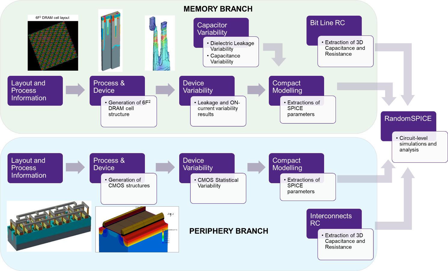
The Synopsys TCAD platform [17–23] is used for the generation and simulation of the 3D DRAM array. The DRAM structures are constructed by means of Process Explorer [17] starting from a 6F2 tilted-cell layout representative of a 2z nm technology node (Figure 2). A single cell and two adjacent neighbors are then cut-out to perform accurate doping implantation and device simulation by means of S-Process [18] and S-Device [19], respectively. Different process conditions are simulated by changing WLetch (WL recess etch) and Dose (roll-off) parameters by +/- 20% (Figure 2) to generate a range of structures corresponding to different process conditions, or process variations. The cell transistor, consisting of a saddle-fin featuring buried metal WL and shared common BL (Table 2), is then re-meshed to enable the statistical simulation of ON and leakage currents by means of the drift-diffusion variability engine Garand VE [20].
It has been previously shown that discrete doping can play a fundamental role in determining the stochastic dispersion of both drive current and leakage current in transistors. In this work, we consider the trap-assisted band-to-band tunneling (TAT) as the dominant contribution to the transistor leakage. The experimental results, in fact, clearly show that the transistor leakage current is a function of the number of defects in silicon, their energy level in the bandgap, and the electric field [6]. The trap-assisted contribution is modelled through an enhancement of the trap capture cross-section in the conventional Shockley-Read-Hall (SRH) generation term. The enhancement can either be computed by Hurkx-like local models or by non-local tunneling path approaches. For each process corner, Garand VE simulates hundreds of statistical instances. Each instance features a different configuration of random discrete dopants (RDD) and thousands of single-trap positions are evaluated to gather the TAT leakage statistics. Once the single-trap leakage statistics are obtained, any other statistics due to an arbitrary trap density can then be obtained at SPICE level by convolution of the single-trap cumulative distribution functions (as detailed in [28]).


Figure 3.   
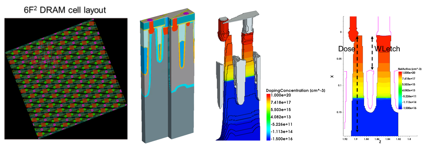
ON current average (left) and variability (right) performance across the space of process variations.


Figure 4.   Leakage complementary cumulative distribution for different process corners (left); the worst leakage value is plotted across the space of process variation (right) as measure of the leakage variability.
Figure 3 shows the results of the Garand VE analysis performed to evaluate the impact of RDD on the ON-current for the DRAM cell, across the WLetch and Dose process variations space. A 10% variation in the mean ON-current can be observed, whilst the ON-current standard deviation varies from 3% to 6% of the nominal ON-current value. These variations can be understood by considering that the combination of WLetch and Dose define the gate to source/drain overlap. With a high WLetch, there is significant underlap, leading to low ON-current and high variability.
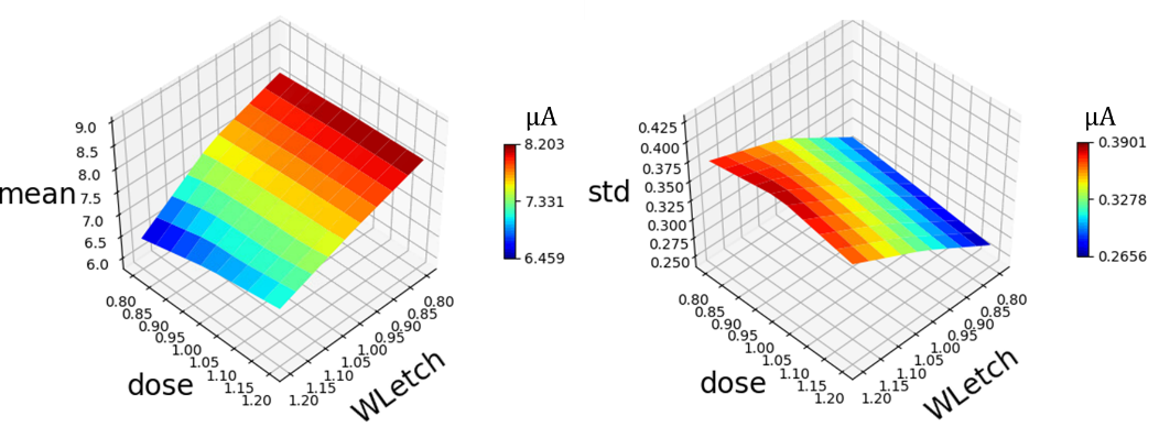
To evaluate the leakage variability, we have performed 200 Garand VE simulations for each process corner. For each RDD configuration, the single-trap TAT leakage is simulated by sweeping the trap position across the drain (storage node contact) pillar region with a 0.5nm spacing, leading to ~70,000 trap evaluations per each RDD configuration (14,000,000 trap configurations for each simulated process condition). Figure 4 shows the leakage complementary cumulative distribution, highlighting that the interaction between discrete traps and random dopants leads to extended exponential-like tails. Moreover, both average and tail behavior strongly depend on the process variations. It is important to note that the variability of ON-current is anti-correlated to the variability of leakage. Therefore, the best process corner that minimizes ON-current variability is also be the worst corner that maximizes leakage variability. This imposes a trade-off between ON-current and leakage performance and, in turn, between DRAM write time (tWR) and tREF performance.
Once the statistical TCAD results are obtained across the space of process variations, compact models can be extracted by means of a response surface methodology in Mystic [21], as detailed and validated in [28]. It is worth remarking that the leakage due to many random traps can be obtained analytically by self-convolution of the single-trap statistics.
3.2. DRAM Capacitor Dielectric Leakage – Statistical Variability
DRAM capacitors utilize high-k dielectrics to maximize capacitance for a given technology node. Defects in high-k materials may cause undesirable leakage currents due to trap assisted tunneling. The leakage currents in the capacitors in a memory device have been one of the bottlenecks for further scaling down. Therefore, a systematic way of modeling and understanding the trap assisted tunneling transport mechanisms is required to support further downscaling.
To calculate the leakage current for a metal-insulator-metal structure, we have developed a stochastic reliability simulator, Sentaurus Device KMC [19], based on the kinetic Monte-Carlo method. The simulator randomly distributes discrete defects in insulator regions of a 3D capacitor structure. These discrete defects act as traps of carriers in an insulator that can affect device reliability. To simulate the electron transport via the traps, the electron hopping event rates are calculated with various physical models [29], including direct tunneling, Fowler-Nordheim (FN) tunneling, inelastic multi-phonon trap-to-trap and trap-to-electrode tunneling [30], and Poole-Frenkel (PF) emission [31]. The direct tunneling and FN tunneling are leakage currents without traps; they are determined by the intrinsic insulator properties. With the traps in an insulator, the inelastic multi-phonon processes dominate the tunneling current. These processes involve the emission and absorption of multiple phonons. In the PF emission, the localized electron in a trap is thermally excited to the conduction band of an insulator. Furthermore, the potential energy distribution is calculated by solving the Poisson equation with the image charge barrier lowering near electrodes as well as the short-ranged trap potentials.
With the KMC method, all possible electron transport events are considered as stochastic process [32]. The steady state current I_k is calculated by counting the net electrons at the electrode ΔN_k within Δt by I_k=(qΔN_k)/Δt, when the stochastic process reaches steady states.
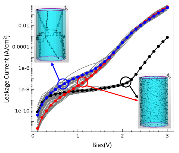
Figure 5 shows the trap assisted tunneling current as a function of the electric field in a HfO2 capacitor. The thickness of the HfO2 layer is 5nm, and the outer diameter of the cylinder is 60nm. The electrodes are TiN. The leakage currents are compared according to the solid states of the insulator, i.e., monocrystalline, amorphous, and polycrystalline HfO2. For the monocrystalline and amorphous HfO2, the traps are randomly distributed in the bulks where the trap concentrations are 2×1019 cm-3 and the trap locations are identical for both structures. For the polycrystalline HfO2, the same number of traps are distributed only on the grain boundaries, which result in smaller trap-to-trap distances in the polycrystalline HfO2. For the crystalline HfO2, a constant trap level, 1.8 eV is used for all traps. In amorphous and polycrystalline HfO2, the trap levels are randomly defined with the Gaussian distribution of the average 1.8 eV and the standard deviation 0.5 eV. In the comparison of the leakage currents in the monocrystalline and amorphous HfO2, the leakage current in the monocrystalline HfO2 is larger than the one in the amorphous HfO2 for low bias, while the leakage current in the amorphous HfO2 becomes larger as the bias increases. For low bias, the inelastic tunneling requires more phonons in the amorphous HfO2 as compared with the monocrystalline HfO2, because the energy differences between the traps are zero in the monocrystalline HfO2. For high bias, the number of phonons for the inelastic tunneling process increases linearly as the electric field increases in the crystalline HfO2, while the tunneling paths requiring fewer phonons can be found in amorphous HfO2 where the trap levels vary over space.
In comparison of the leakage currents in the monocrystalline and amorphous HfO2, the leakage current in polycrystalline HfO2 is larger for the bias below 1.5 V, while the averaged leakage currents are almost identical for both cases when the bias gets higher. For high bias, the single-trap assisted tunneling processes, i.e. electrode-to-trap and trap-to-electrode tunneling, dominate the leakage current. Thus, both leakage currents of amorphous and polycrystalline HfO2 are similar. However, for low bias, in the polycrystalline HfO2, the leakage current is dominated by trap assisted tunneling which is the trap-to-trap tunneling process because of smaller trap-to-trap distances on the grain boundaries. It results in larger leakage current in the polycrystalline HfO2 than one in the amorphous HfO2.
For this simplified example, the capacitor leakage is significantly lower than the transistor leakage, although this may not hold true for more realistic structures and with advanced scaling. Therefore, this KMC analysis represents an important step for the accurate optimization of the DRAM tREF by means of a TCAD-based DTCO platform.


Figure 5.   Leakage current in cylinder capacitors. Black line: Averaged current in the crystalline insulator, traps are randomly distributed in the bulk with the same trap energy of 1.8eV. Red line: Averaged current in the amorphous insulator, traps are randomly distributed in the bulk. Blue line: Averaged current in the polycrystalline insulator, traps are randomly distributed only on grain boundaries.


Figure 6.   
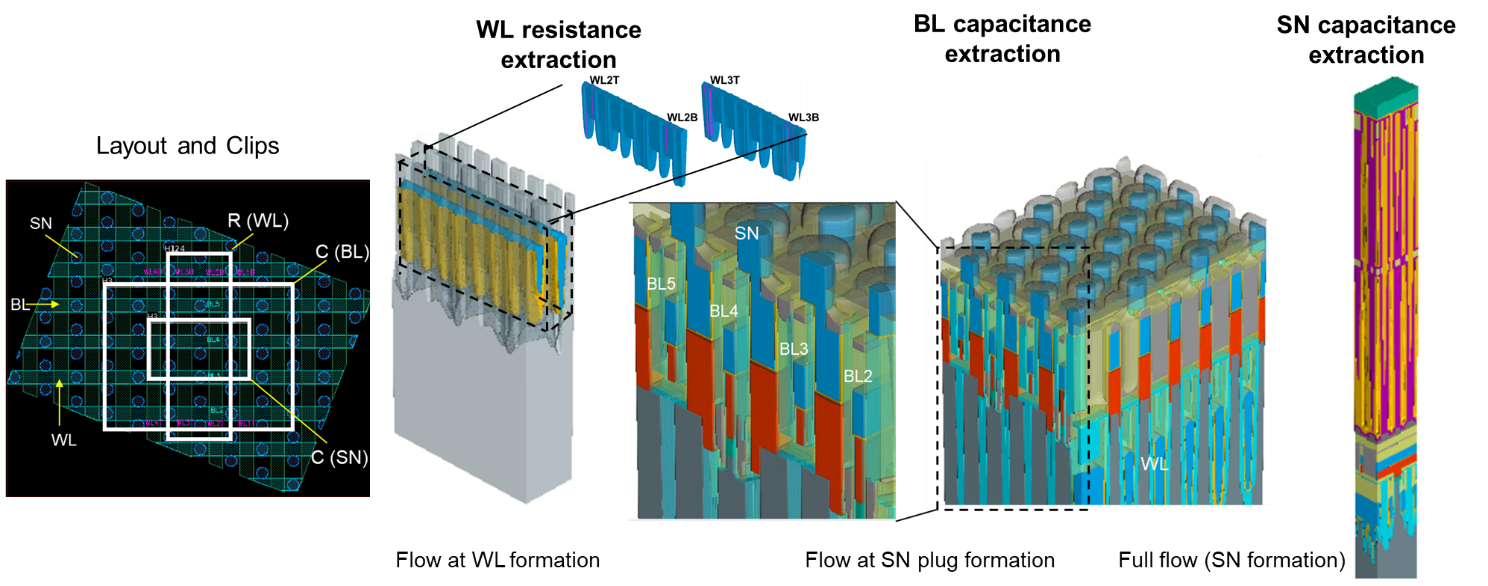
Cell Array RC Extraction. The extraction flow starts from a layout-based structure generation by means Process Explorer. Clips are user-specified to identify the domains of RC extraction, which is then performed by Raphael FX.
3.3.   Cell Array RC Extraction
In the previous sections we have shown how to evaluate the transistor ON-current and leakage and their stochastic dispersions. These TCAD data can be brought to SPICE level via a compact model and a circuit simulation can be performed to obtain outputs such as the DRAM writing time or refresh time. However, this task cannot be achieved without an accurate extraction of the RC parasitics, including bitline (BL) capacitance and the world line (WL) resistance. The cell array capacitance and resistance extraction are performed by using Raphael FX [22], a 3D field solver, therefore offering the highest accuracy for the RC extraction. Moreover, thanks to distributed processing (DP), the tool can keep run-time at optimal levels enabling, for example, the RC extraction of large areas within hours (instead of days). The resistance extraction accuracy is also increased by including surface scattering effect that will lead to an increased resistivity when metal lines cross-sections are scaled down.
Figure 6 shows the cell Array RC extraction flow starting from a layout-based structure generation by means of Process Explorer. Clips are user-specified to identify the domains of the RC extraction, which is then performed by Raphael FX. Table 3 reports single cell capacitance and resistance extracted values. It is worth noting that the BL to SN capacitance dominates the total (~100aF), whilst the BL to BL coupling is relatively weak (~1aF) and the BL to WL coupling is negligible (0.01aF). The WL resistance is around 17 Ohms across the area of extraction. These results will be included in the statistical SPICE analysis presented at the end of Section 4.
4.   Periphery DTCO Analysis
In this section we present a TCAD-to-SPICE methodology for the early SPICE model extraction and performance evaluation of the DRAM CMOS periphery. We will focus our analysis on the Sense Amplifier (SA) circuitry, whose performance will determine the read operation reliability and, ultimately, the tREF margin.
Table 3.   Single-cell Capacitance and Resistance extracted values.
Bit Line Capacitance ExtractionC [F]
BL3BL21.54 ×10-18
BL3BL48.48 ×10-19
BL3BL58.95 ×10-22
BL3SN1.23 ×10-16
BL3WL2T2.03 ×10-20
BL3WL4T2.13 ×10-20
Total Capacitance1.26 ×10-16
Word Line Resistance ExtractionR [Ω]
WL2BWL2T16.9
WL3BWL3T16.8
Global variations could be modeled via different process splits accounting for the systematic variations in implant dose, geometrical dimensions and layout dependent effects – as already presented for the DRAM memory transistor in Section 3. However, because the Sense Amp performance will be mainly determined by the transistor local threshold voltage (Vth) mismatch, in the following we are going to consider only source of local statistical variability. This assumption will not distort the analysis results, unless for that cases where the process variation and local variation are highly correlated. Figure 7 shows the layout-based 3D generation of the DRAM periphery, which is achieved by means of Process Explorer [17]. S-Process [18] is employed for accurate doping and stress simulation, whilst S-Device [19] is used to generate the reference I-V and C-V characteristics that are used for the compact model extraction of the nominal device. A bulk MOSFET technology featuring a nominal gate length of 32nm and a width of 200nm is used a test-bed for this analysis.
4.1. Periphery CMOS Transistors – Statistical Variability
To account for local variability, we deploy the variability engine Garand VE [20]. In a first stage, Garand VE is calibrated against the reference I-V curves from S-Device. This includes density gradient (DG) quantum corrections, inversion charge calibration and mobility model calibration. Then all major sources of local variation are physically modelled by running hundreds statistical instances of the nominal device. These sources include random discrete doping (RDD), line edge roughness (LER) and metal gate granularity (MGG) variability (if metal gate technology) or polysilicon gate granularity (PGG) variability (if polysilicon gate technology) [33]. Figure 8 shows the I-V curves for separate and combined variability sources, highlighting that RDD and MGG play the dominant role in determining the threshold voltage and ON-current variations accounting to 15mv and 0.76µA (@W=0.2um), respectively.
Once all the target I-V/C-V characteristics are generated using physical TCAD simulation, hierarchical compact models can be extracted by means of a two-stage process, involving: i) the extraction of ‘uniform’ or ‘base’ SPICE model; ii) local ‘statistical’ models extraction using a carefully selected subset of the compact model parameters, as detailed in [34]. The results of the extraction are shown in Figure 9 comparing the distribution of key figures of merit obtained from the physical TCAD variability simulation and the extracted statistical compact model.
4.2.   Periphery CMOS Interconnects – RC Extraction
Similarly to the methodology performed for the RC extraction of the DRAM cell array, Raphael FX [22] is deployed to extract the interconnect RC for the 3D structure generated by Process Explorer [17] (Figure 7). The output is a RC netlist in a SPICE-ready format which can be imported, together with the transistor models, into the statistical circuit simulator RandomSpice [23]. Table 4 shows only few lines of the extracted RC netlist.


Figure 7.   Layout to Process and Device simulation for the CMOS periphery Sense Amplifier. A 32nm bulk technology is considered in this example.


Figure 8.   TCAD variability analysis considering separate and combined variability sources (RDD, LER, MGG). Results are for a width of W=25nm. The Sense Amplifier will have transistors featuring W=200 and the variability will be scaled inversely proportional to sqrt(WL).


Figure 9.   Compact Modelling extraction for NMOS and PMOS (RDD, LER and MGG combined). TCAD data in black and compact model results in red.
Table 4.   Sense Amp Interconnect Capacitance and Resistance extracted values.
Capacitance Extraction for SPICEC [F]
C_19_5
C_3_20
C_6_18
SEB
BLB
PG1
nmT23
0mT25
2mT26
6.02 ×10⁻¹⁹
6.97 ×10⁻¹⁹
5.31 ×10⁻¹⁸
Resistance Extraction for SPICER [Ω]
R_0_1
R_2_3
ng20nmT181.50
IIUW2UT24BLB3.79
R_17_6ng1pg129.2
4.3.   Statistical Circuit Analysis
The simulated TCAD data is propagated into statistical SPICE models via the compact modelling extraction presented in the previous sections. The metal lines capacitive and resistive element are also added to the final netlist. For each Monte-Carlo instance of the DRAM cell, a unique leakage current is generated using the fitted TCAD data distributions. These randomized leakage values are converted to BSIM4 junction leakage parameters. The leakage compact models can reproduce the statistical TCAD data at arbitrary trap densities and storage node voltages, as verified in [28]. It is worth to remark that RandomSpice [23] directly generates the leakage values for the DRAM transistor: because we are focusing on a statistical tail analysis, the HSPICE [24] simulations can be limited to the circuits where the DRAM cell leakage current is greater than a threshold limit (here >1 fA). As a result, only ~400k out of 10M generated circuits (representing roughly 10Mbit) are run through HSPICE – enabling a very accurate, yet efficient, high-sigma analysis.
To approximate tREF through SPICE simulation, we combine the output from the SA analysis with DRAM cell analysis. The SA variability is important as it defines how much differential is required between the sensing BL and the reference BL. Local MOSFET mismatch can “offset” a SA towards one state or another, and the natural solution to this is to utilize larger devices in this circuit. However, a larger SA means that proportionally, less of the wafer area is memory cells, reducing overall memory density and increasing cost.
Utilizing the variability aware SPICE models previously extracted we can explore the tradeoff between device width and SA offset voltage as show in Figure 10(left). In this case we select a W=200nm SA design, which leads to 48mV 3σ offset. We can then determine the minimum storage capacitor voltage required to produce a 48mV delta in the BL voltage. In this case, as shown in Figure 10(right), 0.78V must be present on the storage capacitance in order for the ‘1’ state to be correctly detected by a 3σ sense amp. Finally, this voltage can be plugged into the write-and-hold DRAM cell simulations.
Initial simulations, in Figure 11 (left) show the output of a 1e7 sample of cells, where process conditions are kept “nominal”. Here the only variations which are applied relate to RDD and RDD+TAT interactions, and tREF at 1e-7 probability comes out at ~200ms. Finally, we also randomize process conditions for the DRAM cell – in this case this is in the form of (Dose, WLetch) variation. Each datapoint here corresponds to a 1e-7 probability cell, mixed with a 3σ sense-amp to extract a tREF distribution per-10Mb array. The results, in Fig 11 (right) show that, although nominal 10Mb array tREF is ~200ps, array to array tREF 1σ is ~15ms. Although the resultant tREF large compared to reported tREF values– it is worthwhile noting that this analysis was performed at 27C, and not worst-case temperature, where tREF time can easily drop by a significant factor up to 0.3, when shifting from 27C to 80C [35]. Final, these results can be compared to tREF/yield specifications for the process – if yield targets are not achieved, updates in the design may be considered. For example, resizing or redesigning of the sense-amp, to reduce the BL differential requirements and increase tREF can be quantitatively evaluated. This, and other process updates can be quickly evaluated by rerunning the flow with updated inputs.


Figure 10.   (left) Sense-amp offset analysis, showing offset vs. nMOS/pMOS device size. (right) Determination of minimum storage node voltage required to correctly sense the ‘1’ state of the capacitor.


Figure 11.   (left) tREF tail at a nominal process condition, showing how long it takes for Vsnc to drop to 0.78V. (right) Distribution of tREF produced at 1,000 different random process conditions – effectively measuring tREF from 1,000 ~10Mb arrays.
5.   Conclusions
The semiconductor industry is facing a paradigm shift, with scaling being now driven by more frequent technology releases for both memory and logic. DTCO methodology becomes the key to unlock the potential of each release, by means of the efficient and accurate exploration of different technological variations and the optimization of fundamental figures of merit such as Power-Performance-Area-Cost, memory cell retention time, and parametric yields. In this paper we have presented a DTCO analysis of an advanced DRAM technology, aiming at the optimization of the DRAM refresh time. In particular, we have shown how the several components affecting the memory and the logic part can be captured by a multi-stage simulation approach including both process and statistical variations. This enables a variability-aware DTCO particularly suited for optimizing performance and yields of advanced memory technologies, reducing manufacturing cost and cycle time and accelerating time-to-market.
Acknowledgments
[1] V. Moroz, X.-W. Lin, T. Dam, “Logic Block Level Design-Technology Co-Optimization is the New Moore's Law”, 2020 4th IEEE Electron Devices Technology & Manufacturing Conference (EDTM).
[2] P. Matagne, H. Nakamura, M.-S. Kim et al., “DTCO and TCAD for a 12 Layer-EUV Ultra-Scaled Surrounding Gate Transistor 6T-SRAM”, 2018 International Conference on Simulation of Semiconductor Processes and Devices (SISPAD).
[3] A. Asenov, B. Cheng, X. Wang et al., “Variability Aware Simulation Based Design- Technology Cooptimization (DTCO) Flow in 14 nm FinFET/SRAM Cooptimization”, IEEE Transaction on Electron Devices, pp.1682-1690, vol.62, 2015.
[4] Z. Zhang, R. Wang, C. Chen et al., “New-Generation Design-Technology Co-Optimization (DTCO): Machine-Learning Assisted Modeling Framework”, 2019 Silicon Nanoelectronics Workshop (SNW).
[5] A. Asenov, K. El Sayed, R. Borges et al., “TCAD based Design-Technology Co-Optimisations in advanced technology nodes”, 2017 International Symposium on VLSI Technology, Systems and Application (VLSI-TSA).
[6] S.C. Song, B. Colombeau, M. Bauer et al., "2nm Node: Benchmarking FinFET vs Nano-Slab Transistor Architectures for Artificial Intelligence and Next Gen Smart Mobile Devices", Symposium on VLSI Technology, pp. 206-207, 2019.
[7] J. X. Niu, H. Veluri, A. V.-Y. Thean, “Design-Technology Co-optimization (DTCO) for Emerging Disruptive Logic & Embedded Memory Process Technologies”, 2019 Electron Devices Technology and Manufacturing Conference (EDTM).
[8] Y. Kim, U. Monga, J. Lee et al., “The efficient DTCO Compact Modeling Solutions to Improve MHC and Reduce TAT”, 2018 International Conference on Simulation of Semiconductor Processes and Devices (SISPAD).
[9] I. Jang, H. Ko, A. Schmidt et al., “Multi-domain process modeling for advanced logic and memory devices: from equipments to materials”, 2018 IEEE International Electron Devices Meeting (IEDM).
[10] S.-H. Lee, “Technology scaling challenges and opportunities of memory devices”, 2016 IEEE International Electron Devices Meeting (IEDM).
[11] S.-W. Park, S.-J. Hong, J.-W. Kim et al., “Highly Scalable Saddle-Fin Transistor for Sub-50nm DRAM Technology”, 2006 Symposium on VLSI Technology, 2006. Digest of Technical Papers.
[12] S.-W. Ryu, K. Min, J. Shin et al; “Overcoming the reliability limitation in the ultimately scaled DRAM using silicon migration technique by hydrogen annealing”, 2017 IEEE International Electron Devices Meeting (IEDM).
[13] C.-M. Yang, C.-K. Wei, Y. J. Chang et al; “Suppression of Row Hammer Effect by Doping Profile Modification in Saddle-Fin Array Devices for Sub-30-nm DRAM Technology”, IEEE Transactions on Device and Materials Reliability, pp. 685-687, vol.16, 2016.
[14] S. H. Jang, J. Lim, J. Han et al., “A Fully Integrated Low Voltage DRAM with Thermally Stable Gate-first High-k Metal Gate Process”, 2019 IEEE International Electron Devices Meeting (IEDM).
[15] S-K Park, “Technology Scaling Challenge and Future Prospects of DRAM and NAND Flash Memory”, 2015 IEEE International Memory Workshop (IMW).
[16] M. H. Cho, N. Jeon, T. Y. Kim et al., “An Innovative Indicator to Evaluate DRAM Cell Transistor Leakage Current Distribution”, IEEE Journal of the Electron Devices Society, pp. 494-499, vol. 6, 2018.
[17] Process Explorer User's Manual v. R-2020.09 Synopsys, 2020.
[18] Sentaurus Process User's Manual v. R-2020.09 Synopsys, 2020.
[19] Sentaurus Device User's Manual v. R-2020.09 Synopsys, 2020.
[20] Garand VE User's Manual v. R-2020.09 Synopsys, 2020.
[21] Mystic User's Manual v. R-2020.09 Synopsys, 2020.
[22] Raphael FX User's Manual v. R-2020.09 Synopsys, 2020.
[23] RandomSpice User's Manual v. R-2020.09 Synopsys, 2020.
[24] HSPICE User's Manual v. R-2020.09 Synopsys, 2020.
[25] A. Ghetti, C. Monzio Compagnoni, L. Digiacomo et al., “Evidence for an atomistic-doping induced variability of the band-to-band leakage current of nanoscale device junctions”, 2012 International Electron Devices Meeting.
[26] T. Yang, X.-W. Lin, “Trap-Assisted DRAM Row Hammer Effect”, IEEE Electron Device Letters, pp. 391-394, vol. 40, 2019.
[27] I. Ciofi, P. J. Roussel, C. J. Wilson et al., “Variability-Aware Predictive Modeling of Line-to-Line Dielectric Reliability”, IEEE Transactions on Electron Devices, pp. 1737-1744, vol. 67, 2020
[28] S. M. Amoroso, J. Lee, P. Asenov et al., “High-sigma analysis of DRAM write and retention performance: a TCAD-to-SPICE approach”, 2020 International Conference on Simulation of Semiconductor Processes and Devices (SISPAD).
[29] G.C. Jegert, “Modeling of Leakage Currents in High-k Dielectrics,” Ph.D. Thesis, Technishen Universität München, Sept 9, 201l.
[30] M. Herrmann and A. Schenk, “Field and High-temperature Dependence of the Long Term Charge Loss in Erasable Programmable Read Only Memories: Measurements and Modeling,” J. Appl.Phys., vol. 77, no. 9, pp. 4522-4540, May 1995.
[31] J. Frenkel, “On pre-breakdown phenomena in insulators and electronic semiconductors”, Physical Review., vol. 54, no. 8, pp. 647–648, 1938.
[32] L. Vandelli, A. Padovani, L Larcher et al., “Microscopic Modeling of Electrical Stress-Induced Breakdown in Poly-Crystalline Hafnium Oxide Dielectrics”, IEEE Transactions on Electron Devices, vol. 60, pp. 1754-1762, 2013.
[33] A. Cathignol, B. Cheng, D. Chanemougame et al., “Quantitative Evaluation of Statistical Variability Sources in a 45-nm Technological Node LP N-MOSFET”, IEEE Electron Device Letters, vol. 29, 2008.
[34] X. Wang, B. Cheng, D. Reid et al., "FinFET Centric Variability-Aware Compact Model Extraction and Generation Technology Supporting DTCO", IEEE Transactions on Electron Devices, vol. 62, pp. 3139-3146, 2015.
[35] J. Liu, B. Jaiyen, Y. Kim, C. Wilkerson, O. Mutlu, “An experimental study of data retention behavior in modern DRAM devices: implications for retention time profiling mechanisms” ISCA 2013, Proc. of the 40th Annual International Symposium on Computer Architecture, pp. 60-71, 2013
Xi-Wei Lin is Business Development Director from Silicon Engineering Group in Synopsys, currently focusing on TCAD and DTCO applications for logic and memory technology developments.  He previously worked at Micron Technology, LSI Logic, Philips Semiconductors, and Lawrence Berkeley National Laboratory, responsible for materials science and engineering, CMOS process technology development, ASIC and memory designs and verification, as well as power methodology and standard cell library architecture.  He received his B.S. degree in microelectronics from Beijing University, China and M.S. and Ph.D. in solid state physics from University of Paris, Orsay, France.
Article and author information
Salvatore M. Amoroso
Salvatore Maria Amoroso received his Ph.D. in Electronic Engineering from Politecnico di Milano in 2012. He has been with the Device Modelling Group of University of Glasgow as a Research Associate, working on the advanced simulation of variability and reliability of decananometer MOSFETs and Flash Memories, until 2014. He joined Gold Standard Simulations Ltd, in 2014 working as a Senior Engineer for TCAD software development and customer accounts manager. Since 2016 he is with Synopsys, Inc. working as an R&D Engineer on the development of advanced TCAD-to-SPICE methodologies and Design-Technology Co-Optimization (DTCO) enablement.
Plamen Asenov
Plamen Asenov received is PhD from Glasgow University in 2012. He has been with ARM, where he worked on embedded memory design at advanced nodes until 2015. He joined Gold Standard Simulations in 2015, working on DTCO applications. Since 2016 he has been with Synopsys as an R&D Engineer, specializing in TCAD-to-SPICE and DTCO across a range of technologies.
Jaehyun Lee
Jaehyun Lee has been with SK Hynix from 2008 to 2012 as Research Engineer for mobile DRAM development. He received his Ph. D. in Electrical Engineering from Korea Advanced Institute of Science and Technology in 2016. He joined Device Modelling Group of University of Glasgow, working as a Research Associate on the software development of interconnect and nanoscale MOSFETs. Since 2018, he is with Synopsys working as an R&D Engineer on the development of TCAD-to-SPICE and Design-Technology Co-Optimization (DTCO) methodologies.
Nara Kim
Nara Kim has received the B.S degree in physics from Konkuk University, Seoul, South Korea, in 2009. She has been with Semiconductor Research and Development Center, Samsung Electronics Company Ltd., Hwaseong, South Korea as TCAD engineer to research on the development of the semiconductor device from 2009 to 2019. Since 2019 she has been with Synopsys, Inc. working as an Application Engineer.
Ko-Hsin Lee
Yong-Seog Oh joined Daewoo Telecom in Korea to develop BiCMOS technology as soon as he received B.S. in physics from Seoul National University in 1987. He led the team for TCAD simulation and SPICE parameter extraction as well as the test pattern design including ESD protection. In 1994, he moved to US to join Stanford spin-off Technology Modeling Associates (TMA) as an R&D engineer for the process simulator, TSUPREM-4. After IPO in 1997, TMA became a part of Avant! in 1998 and of Synopsys in 2002. He accomplished many projects on process and material model development until 2019. His current main concern is on the device reliability, topography modeling and calibration for the state-of-art semiconductor process.
Yaohua Tan
Yong-Seog Oh
Lee Smith
Lee Smith received the B.S. degree in physics from the University of Florida and the Ph.D. degree in physics from Stanford University. Dr. Smith is currently R&D manager of the TCAD Device Simulation group at Synopsys which is engaged in the development of advanced device modeling techniques for a variety of applications including CMOS, power, RF, and memory devices.
Xi-Wei Lin
xiwei@synopsys.com
Xi-Wei Lin is Business Development Director from Silicon Engineering Group in Synopsys, currently focusing on TCAD and DTCO applications for logic and memory technology developments. He previously worked at Micron Technology, LSI Logic, Philips Semiconductors, and Lawrence Berkeley National Laboratory, responsible for materials science and engineering, CMOS process technology development, ASIC and memory designs and verification, as well as power methodology and standard cell library architecture. He received his B.S. degree in microelectronics from Beijing University, China and M.S. and Ph.D. in solid state physics from University of Paris, Orsay, France.
Victor Moroz
Victor Moroz received M.S. degree in Electrical Engineering from Novosibirsk Technical University and Ph.D. degree in Applied Physics from the University of Nizhny Novgorod. After engaging in technology development at several semiconductor manufacturing companies and teaching semiconductor physics at a University, Dr. Moroz joined a Stanford spin-off Technology Modeling Associates in 1995. After IPO in 1997, the TMA TCAD team became part of Avanti in 1998, and in 2002 it became a key part of Synopsys, connecting a synthesis company to the manufacturing. Currently Dr. Moroz is a Synopsys Fellow, engaged in a variety of projects on modeling advanced CMOS with over 100 US patents, and serving as an Editor of IEEE Electron Device Letters.
Publication records
Published: Dec. 30, 2020 (Versions2
References
Journal of Microelectronic Manufacturing