Research Article Current Issue Versions 2 Vol 3 (4) : 20030407 2020
Download
Fast and Accurate Machine Learning Inverse Lithography Using Physics Based Feature Maps and Specially Designed DCNN
: 2020 - 09 - 28
: 2020 - 12 - 15
: 2020 - 12 - 30
2709 38 0
Abstract & Keywords
Abstract: Inverse lithography technology (ILT) is intended to achieve optimal mask design to print a lithography target for a given lithography process. Full chip implementation of rigorous inverse lithography remains a challenging task because of enormous computational resource requirements and long computational time. To achieve full chip ILT solution, attempts have been made by using machine learning techniques based on deep convolution neural network (DCNN). The reported input for such DCNN is the rasterized images of the lithography target; such pure geometrical input requires DCNN to possess considerable number of layers to learn the optical properties of the mask, the nonlinear imaging process, and the rigorous ILT algorithm as well. To alleviate the difficulties, we have proposed the physics based optimal feature vector design for machine learning ILT in our early report. Although physics based feature vector followed by feed-forward neural network can provide the solution to machine learning ILT, the feature vector is long and it can consume considerable amount of memory resource in practical implementation. To improve the resource efficiency, we proposed a hybrid approach in this study by combining first few physics based feature maps with a specially designed DCNN structure to learn the rigorous ILT algorithm. Our results show that this approach can make machine learning ILT easy, fast and more accurate.
Keywords: Optimal feature maps; inverse lithography technology (ILT); deep convolution neural network (DCNN)
1.   Introduction
Semiconductor industry has been progressed continuously from node to node to meet the ever increasing demand on chip performance improvement, power consumption reduction and cost reduction. The technology advancement has been enabled by various innovations in relevant fields, including new lithography exposure tools, new materials, new device architectures and new process technologies. The enormous challenges in the building of EUV lithography infrastructure has not slowed down the industry in the past, instead, the gap left by the difference in hardware resolution capability between immersion exposure tools and EUV exposure tools had created opportunities for the development and adoption of computational lithography technologies. We have witnessed the adoption of sub-resolution assist features (SRAF), multiple patterning technologies (MPT), and the source-mask co-optimization (SMO). The computational lithography technologies mentioned above have become the standard practice in developing integrated lithography patterning solutions for advanced semiconductor technology nodes. Source-mask co-optimization realizes the optimal lithography process for a selected set of patterns derived from a given set of pattern design rules. With the illumination source obtained from SMO, the lithograph process window of a chip for a design layer depends mainly on the quality of optical proximity correction (OPC) solution, which relies on the placement quality of SRAFs to a very large extent. The placement of SRAFs has gone through several evolutions, from simple rule based placement to model derived template placement, to inverse lithography technology (ILT) produced placement in hotspots fixing loop. In theory, inverse lithography has provided solid mathematical framework for achieving optimal mask solution. Although rigorous inverse lithography algorithms do exist in various forms [1, 2], full chip rigorous inverse lithography solution remains a challenging task in practice. Realization of full chip inverse lithography is not an academic interest only; it has enormous practical significance for advanced lithography process for tight pattern edge placement error control, in particular, for EUV lithography process for which stochastic effect induced edge placement error is significant. The effective way to reduce EUV lithography process stochastic effect is to improve image contrast through optimal assist feature placement.
The research and development in ILT has achieved fruitful progress in two directions recently. In one direction, a breakthrough has been reported in full chip rigorous mask 3D simulations through intelligent and efficient algorithm that gains computational acceleration from arrays of GPUs [3, 4]. In another direction, machine learning ILT based on deep convolution neural network (DCNN) has also been explored with success [5, 6]. Machine learning ILT is not aimed at replacing rigorous ILT entirely, instead, machine learning ILT is intended to offer sufficiently good initial ILT solution for rigorous ILT engine to take over to reach convergence with extremely fast computational speed. In essence, machine learning ILT solution can be viewed as constructing a nonlinear mapping function between the lithography target design and the rigorous ILT solution. It is not a simple point-to-point mapping; it is a function-to-point mapping. Machine learning ILT is made up of three major parts: (1) feature vector design; (2) neural network design, (3) machine learning ILT model training strategy. Feed-forward multilayer neural network architecture has been proven to possess the capability of constructing function-to-point mapping [7,8]; while convolution network has the capability of exploring spatial correlation hierarchically and extracting feature vector representation automatically through training. In semiconductor industry, DCNN has been applied to hot spot detection as a classification problem [9, 10, 11, 12] to ILT solution as a regression problem [5, 6]. However, previous implementation of DCNN for ILT uses rasterized lithography target design as input, with such pure geometrical image as input, the feature vectors extracted from DCNN lack of intuitive physical interpretation, they cannot address the critical questions regarding feature vector design, i.e., the feature vector resolution, the feature vector sufficiency, and the feature vector efficiency. The optimality of the feature vector extracted from such DCNN implementation is much more sensitive to the training samples selected.
In our previous reports, we have presented our machine learning OPC and machine learning ILT results based on physically derived feature vector design followed by a shallow (5 to 6 layers) feed-forward neural network [13, 14]. For machine learning ILT with our proposed physically derived feature vector design, the feature vector length needs to be around 140 to achieve satisfactory model accuracy, which will demand considerable memory resource in practical implementation. To lift the memory resource burden while still taking advantage of physics based feature vector design, we propose a hybrid approach in this study, which uses first few physics based feature maps as input, followed by a specially designed DCNN. The specially designed DCNN possesses the desired properties of being wide receptive field and of being able to preserve high resolution. It turns out that this hybrid approach can make machine learning ILT easy, fast and more accurate.
2.   Feature Vector Design for Machine Learning ILT
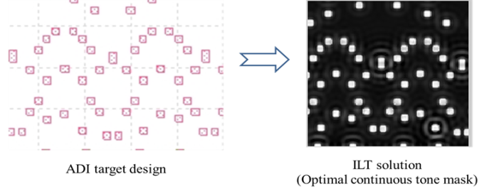
Machine learning based ILT can be generally stated as: For a given ADI target layer and a fixed optimal mask generation mechanism (illumination source + mask type + rigorous ILT algorithm), there should exist a unique mapping function between ADI target data and ILT data, as shown in Figure 1.


Figure 1.   Mapping from ADI target to ILT image.
Mathematically,it can be expressed as
(1)
As we emphasized earlier, it is not a point-to-point mapping, it is a function-to-point mapping. The value of ILT solution at point (x, y) not only depends on the value of ADI target data at point (x, y), but also depends on all values of ADI target data around the point (x, y) within an influence range. Before we proceed to address the question of how to design feature vector to describe the neighboring environment around a point (x, y), we should first ask the question: how many degrees of freedom does the neighboring environment around a point (x, y) have? The theoretical answer is: the degree of freedom of the neighboring environment around a point (x, y) is infinite. Therefore, a complete description of the neighboring environment around a point (x, y) is impossible. Fortunately, a description with infinite resolution is often not required practically. This is true for machine learning based computational lithography, because the imaging system used in lithography process does not possess infinite resolution. This fact suggests that the number of effective degree of freedom of the neighboring environment around any point (x, y) can be considered finite practically. This observation and fact is the very foundation of all computational lithography. The second question we need to address is: what is a feature vector and what desired properties a feature vector should have? Essentially, a feature vector is a mathematical representation that describes the neighboring environment around a point (x, y) in a quantitative way. As a measurement device, a feature vector must address the following important properties, i.e., the measurement resolution, the measurement sufficiency (completeness), and the measurement efficiency. In addition, it is very desirable for a feature vector to possess a property such that the mapping function from input to output of the neural network model is less nonlinear and smooth (differentiable), or even monotonic (hopefully).
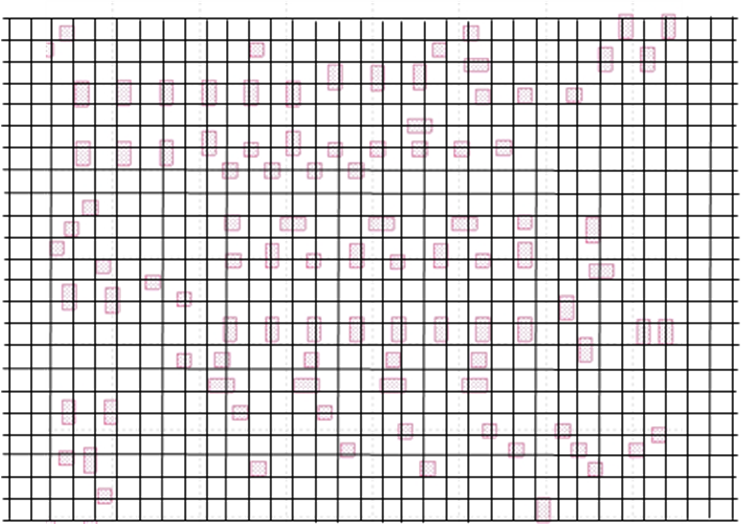

Figure 2.   Divide the neighboring environment into cells.
To elucidate the concept of measurement resolution and measurement efficiency of a feature vector, we can look at Figure 2. To describe the neighboring environment around a point (x, y), we can divide the influencing area into small cells. Assume the influencing range is 1.0 μm each side, and the cell size is x nm, then the cell size x determines the resolution of the feature vector representation, and the total number of cells = (2·1000/x)2 represents the maximum length of the feature vector for a complete description with resolution x nm. Clearly, the smaller the cell size x, the higher the measurement resolution; and the higher the resolution of the feature vector representation, the longer the feature vector is. To serve the machine learning based ILT properly, the resolution of the feature vector representation must meet a minimum requirement, which is determined by lithography process imaging condition, i.e., cell size x = k·λ/(NA(1+σmax)). The k coefficient is related to the degree of spatial coherence of the illumination, which depends on the effective illumination area of the source. A typical cell size for high NA immersion lithography process is around 15nm to 20nm, therefore, the estimated feature vector length for a complete description is (2000/20)2 = 10000. Of course, such a simple and plain encoding scheme for neighboring environment lacks of efficiency, because the encoding scheme does not explore the characteristics of the lithography process, it treats all cells equally and independently, it does not explore all symmetry properties among all the cells. Intuitively, not every cell has the same influence on the point of interest, on average, the closer the cell to the point of interest, the more important the cell is. As to the sufficiency of a feature vector, it is related to the capability of the feature vector in describing the neighboring environment completely within allowed error bound. Simply stated, for any two feature vectors X1 , X2 , if X1 = X2 , then, the condition |F (X1 ) - F (X2 )| ≤ ε (ε is the allowed error bound related to data noise) CANNOT be violated.
There have been several reported ways of designing feature vectors for computational lithography. Incremental concentric square sampling [15], incremental concentric circle area sampling [16], polar Fourier transform [17] have all been proposed to be used for constructing feature vectors for computational lithography. These feature vector designs do not address the optimality of the designed feature vector, and most of them are pure geometrical based feature vectors, except the design based on polar Fourier transform. Feature vectors based on “geometrical rulers” have intrinsic deficiency in machine learning computational lithography; this is particularly true for inverse lithography which grows assist features out of blank areas in mask space. As it is known, rule based assist feature insertion based on geometrical measurement has abrupt change points in the rule table. Therefore, machine learning inverse lithography using “geometrical ruler” based feature vector as neural network input must possess more complicated network structure to learn those abrupt change points in order to map the feature vector into correct response function domain. Feature vectors derived from polar Fourier transform made progress by exploring the characteristics of the lithography process partially, however, it still fails to fully take the imaging process physics into account. Feature vector design is essentially an information encoding scheme design. For machine learning computational lithography, there are three spaces we can use for information encoding, the lithography target space, which is pure geometrical; the mask space, which has geometrical information and optical property information; the image space, which contains information about design geometries, mask optical properties and imaging formation characteristics. From an information point of view, information in lithography target space is not complete (without specifying optical properties of the background and the pattern covered areas), if feature vector design is in lithography target space, then the subsequent DCNN must learn mask optical properties, nonlinear imaging formation process and rigorous ILT algorithm. Information in mask space is complete and of highest resolution. If feature vector design is in mask space, then the subsequent DCNN must learn nonlinear imaging formation process and rigorous ILT algorithm. Information in imaging space can be used to recover information in mask space fully within the resolution limit defined by optical imaging condition. If feature vector design is in image space, then the subsequent DCNN only need to learn the rigorous ILT algorithm. Between mask space and image space, which space is narrower in terms of encoding efficiency? In mask space, the “function space” is constrained by design rules of the layer; while in image space, the “function space” is constrained by both design rules and imaging conditions. Stated explicitly, all aerial images derived from a given imaging condition constitute a special class of functions. In other words, the “function space” in image space is narrower than the “function space” in mask space, and the information lost in image space in comparison with that in mask space is beyond the optical imaging resolution. Therefore, optimal feature vector design for computational lithography should be related to optimal and efficient representation of aerial images of the class at hand.
Now the question becomes how to represent aerial images most efficiently?The aerial image function I(x,y) is a band-limited function. While a real function with finite bandwidth Ω can always be represented by a set of basis functions of the same bandwidth, there still exists the question whether there is an optimum set of basis functions among all the possible sets of basis functions with bandwidth, Ω. By the optimum set of basis functions, it means that only the minimum number of the basis functions that are needed to approximate any real valued function of bandwidth, Ω, for a specified error requirement. To seek the optimal representation of aerial image function, we can refer to the imaging equation of Hopkin’s, which can be decomposed into a sum of coherent imaging system for partially coherent illumination, as shown in Equation (2) below.
(2)
where ⊗ represents the convolution operation between the ith kernel and the mask transmission function M. {Φi} and {αi} are the set of eigenfunctions and eigenvalues of the transmission cross coefficients matrix (TCCs). This optimal imaging system decomposition is originally designed for fast aerial image calculation under partial coherent illumination, and it has been proved that this decomposition scheme is the optimal decomposition in terms of computational efficiency 
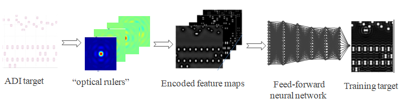
[18]. From an information theory point of view, we can interpret it as an optimal and most efficient aerial image information encoding scheme. This suggests that imaging system kernels {Φi} captures imaging system characteristics fully, and they are a set of natural and optimal “optical rulers” for measuring or estimating the neighboring environment around a point (x, y), because the set of {Φi} eigenfunctions are orthonormal functions. Based on the above reasoning, we define {S1 , S2 , … , SN } as the feature vector, with Si being defined as
(3)
Then, the machine learning inverse lithography problem can be reformulated from Equation (1) to Equation (4).
(4)
The idea of using imaging eigen signal set {Si } to describe aerial image has been used previously for OPC model and lithography two-dimensional patterns’ quantification [19, 20]. Now we turn to the question of how to obtain the approximate function 
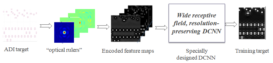
F, this is related to neural network design.
3.   Machine Learning Based ILT and Results
With feature vectors calculated using Equation (3), a general mapping function described by Equation (4) can be constructed using a feed-forward neural network structure, as suggested by the universal approximation theorem [7, 8]. The results based on this approach have been reported in our previous report [14]. Figure 3 shows the key elements of the approach.


Figure 3.   Feed-forward neural network model.
Since both the input feature vector maps and the output (continuous tone mask) are band-limited functions, they are smooth and differential functions. This property makes the mapping function construction easier using feed-forward neural networks. However, we found that the required feature vector is still considerably long in size (140 elements in our study) in order to achieve good model. This will impose considerable requirement on memory resource in practical applications. To ease the memory resource requirement while keeping physics based feature vector as input, we have taken a hybrid approach in this study. In this hybrid approach, we used {S1, S2, S3, S4, S5} five feature maps as input into a specially designed deep convolution neural network (DCNN). The basic idea is to use first few physics based feature maps, which are supposed to be able to provide sufficient information to represent mask optical properties and imaging process characteristics, then the subsequent DCNN to develop more deeper and efficient representation for ILT modeling and to accomplish coordinated regression. This is because both input feature maps and the output image (continuous tone mask) have certain degree of spatial correlation, i.e., neighboring pixels are correlated. To serve machine learning inverse lithography purpose, the specially designed DCNN structure should possess certain desired properties: (1). The wider the receptive field, the better, in order to explore the spatial information around a point (x, y); (2). The original resolution of the image should be preserved; (3). The depth of the DCNN should be moderate, so that there will be no need to have residual connections in the network structure for easy training. Following these design guidelines, we replace all pooling layers with bath normalization layers, and we use ReLU as the activation function. The convolution kernels are all 3x3 in size, and the stride step size is 1. The design of our hybrid approach is shown in Figure 4.


Figure 4.   Hybrid approach machine learning inverse lithography model.
The training of the neural network model needs to include training samples and test samples, and they are selected from the periphery areas of a 28nm SRAM design via layer. The pattern selection strategy is the same as that for OPC model calibration and SMO. Total number of images for training is 134, and total number of images for model test is 48. We have tried both He initialization and orthogonal initialization for weights in model training, and we found there is no essential difference in terms of the model quality from these two different weight initialization schemes. The learning rate used is 5x10⁻⁵, and Adam optimizer is used in training.
To assess the model quality, we first normalize the rigorous inverse lithography solution into [0, 1] using a common normalization factor, then we use two metrics to quantify the quality of a model. Let O denote the normalized rigorous inverse lithography solution image, and Ô the neural network model predicted image. Then the first metric we used is the probability P(|OÔ | ≤ ε) where ε = 0.1 and 0.05, and the other metric used is RMSE. For comparison purpose, besides using {S1, S2, S3, S4, S5} as DCNN input, we also used {Aerial image} and {Aerial image + S1:S5} as DCNN input. The model training error statistics and test error statistics are shown in Table 1 below.
Table 1.   Model training error statistics and verification error statistics
Model inputError spec.P(|OÔ | ≤ ε)RMSE (x10-4)
Training setTest setTraining setTest set
Aerial imagesP(|OÔ | ≤ 0.10)0.9870.9763.54.4
P(|OÔ | ≤ 0.05)0.9280.916
{S1:S5}P(|OÔ | ≤ 0.10)0.9990.9951.82.6
P(|OÔ | ≤ 0.05)0.9890.968
Aerial images
+ {S1:S5}
P(|OÔ | ≤ 0.10)0.9980.9891.92.9
P(|OÔ | ≤ 0.05)0.9870.965
The visual comparison between images from rigorous ILT solutions and from our machine learning model for training set and test set are shown in Figure 5 and Figure 6.


Figure 5.   Images from rigorous ILT solutions and from machine learning model for training set, model input: {S1:S5}.


Figure 6.   Images from rigorous ILT solutions and from machine learning model for test set, model input: {S1:S5}.
As it can be seen from Table 1, the first five feature vector maps (images) {S1:S5} are better model input design than aerial image alone. Aerial image is the weighted sum of many signals (images) from independent imaging formation kernels {Φi}, as expressed in Equation (2). The sum operation makes the original information collapse to a certain extent, the set of independent feature vector maps (images) {S1:S5} preserves the original information better. With the first five feature vector maps (images) {S1:S5} as DCNN input, P(|OÔ | ≤ 0.05) can reach 96.8%. This is better than the model performance using feed-forward neural network with long feature vector (feature vector length =140), the feed-forward neural network model can only achieve P(|OÔ | ≤ 0.1) = 99.0% and P(|OÔ | ≤ 0.05) = 87.5%. The improved model accuracy of the hybrid approach proposed in this study may result from a combination of the physics based feature maps, which contain information about the image formation mechanism, and the power of DCNN, which possesses the great capability of further exploring spatial information from {S1:S5} and of constructing deeper representation most suitable for learning rigorous ILT mechanism.
Besides the greatly improved model accuracy in comparison with the feed-forward model, the speed enhancement relative to rigorous ILT is also significant. With 4 CPUs (Intel Xeon E7-8855-V4, 2.1 GHz, each CPU has 14 cores), it takes 12.1 seconds on average for a 20μmx20μm patch. In comparison with rigorous algorithm (assume 100 iterations for reaching convergence), the estimated speed gain factor is about 25 or more. By running the model on a single GPU (Nvidia telsa M60), additional speed enhancement by a factor of 20 can be achieved.
4.   Conclusion
Inverse lithography technologies can theoretically provide the ultimate optimal mask solutions once the lithography process imaging condition is fixed. However, its full chip implementation has been in stagnation for a long time due to its lack of sufficient speed using rigorous algorithms. A hybrid approach by combining machine learning inverse lithography technology with faster rigorous ILT algorithms has paved the way for its full chip implementation. Due to high accuracy requirement, machine learning inverse lithography is not intended to provide the final ILT solution entirely; rather, it provides a sufficiently good initial solution for a rigorous engine to take over and to achieve final converged solution with very few iterations. In our proposed machine learning inverse lithography method, we use information in image space directly instead of information in design geometrical space as model input to lift the burden for the model to learn very non-linear imaging physical process. We also employ a specially designed DCNN that can both develop more efficient representation for machine learning ILT from imaging space information and do coordinated regression. The new innovative method has made machine learning ILT easy, fast and more accurate.
Acknowledgments
[1] A. E. Rosenbluth, S. Bukofsky, C. Fonseca, M. Hibbs, K. Lai, R. N. Singh, and A. K. Wong, “Optimal mask and source patterns to print a given shape”, J. Microlith. Microfab. Microsys. I(1), 13-30 (2002).
[2] L. Pang, Y. Liu, and D. Abrams, “Inverse lithography technology (ILT): a natural solution for model-based SRAF at 45nm and 32nm”, Proc. SPIE, 6607, (2007)
[3] Yeung, M. and Barouch, E., “Development of fast rigorous simulator for large-area EUV lithography simulation.” Proc. SPIE 10957,109571D, (2019).
[4] L. Pang, E. V. Russell, B. Baggenstoss, M. Lee, etc., “Study of mask and wafer co-design that utilizes a new extreme SIMD approach to computing in memory manufacturing – full chip curvilinear ILT in a day”, Proc. SPIE 11148, (2019).
[5] Shibing Wang et al., “Efficient full-chip SRAF placement using machine learning for best accuracy and improved consistency”, Proc. SPIE 10587, (2018).
[6] Song Lan, Jun Liu, Yumin Wang, Ke Zhao, Jiangwei Li, “Deep learning assisted fast mask optimization.”, Proc. SPIE 10587, (2018).
[7] Cybenko, G., “Approximation by superposition of a sigmoidal function.”, Mathematics of Control. Signals and Systems. 2, (1989), 303-314.
[8] Hornik, Kurt, “Approximation Capabilities of Multilayer Feedforward Networks.”, Neural Networks, Vol. 4, (1991), 251-257.
[9] Haoyu Yang, Luyang Luo, Jing Su, Chenxi Lin, and Bei Yu, “Imbalance Aware Lithography Hotspot Detection: A Deep Learning Approach.”, Proc. SPIE 10148, (2017).
[10] Yibo Lin, Xiaoqing Xu, Jiaojiao Ou, David Pan, “Machine Learning for Mask/Wafer Hotspot Detection and Mask Synthesis”, Proc. SPIE 10451, (2017).
[11] Tetsuaki Matsunawa, Shigeki Nojima, and Toshiya Kotani, “Automatic Layout Feature Extraction for Lithography Hotspot Detection Based on Deep Neural Network.”, Proc. SPEI 9781, (2016).
[12] Yiwei Yang, Zheng Shi, Litian Sun, Ye Chen, Zhijuan Hu, “A kernel-Based DfM Model for Process from Layout to Wafer”, Proc. SPIE 7641, (2010).
[13] Xuelong Shi, Yuhang Zhao, Shoumian Chen, Ming Li, “Optimal feature vector design for computational lithography”, Proc. SPIE 10961, (2019).
[14] Xuelong Shi, Yuhang Zhao, Shoumian Chen, Chen Li, “Physics based feature vector design: a critical step towards machine learning based inverse lithography”, Proc. SPIE 11327, (2020).
[15] Gu A. and Zakhor A., “Optical proximity correction with linear regression.”, IEEE Trans. Semicond. Manuf. Vol. 21, (2008), 263-71.
[16] Tetsuaki Matsunawa, Bei Yu and David Pan, “Optical proximity correction with hierarchical Bayes model.”, Proc. SPIE 9426, (2015).
[17] Suhyeong Choi, Seongbo Shim, Youngsoo Shin, “Machine learning (ML)-guided OPC using basis functions of polar Fourier transform.”, Proc. SPIE 9780, (2017).
[18] Y. C. Pati nd T. Kailath, “Phase-shifting masks for microlithography: automated design and mask requirements”, J. Opt. Soc. Am. A. vol. 11 (9), 1994.
[19] Xuelong Shi, Tom Laidig, J. Fung Chen, Doug Van Den Broeke, Stephen Hsu, Michael Hsu, Kurt Wampler, Uwe Hollerbach, “Eigen decomposition based models for model OPC”, Proc. SPIE 5446, (2004).
[20] Xuelong Shi, J. Fung Chen, Doug Van Den Broeke, Stephen Hsu, Michael Hsu, “Quantification of two-dimensional structures generalized for OPC model verification”, Proc. SPIE 6518, (2007).
Article and author information
Xuelong Shi
Xuelong Shi is a technologist in Shanghai IC R&D Center. He has a BS degree in chemistry from University of Science and Technology of China in 1985, and a PhD degree in physical chemistry from Columbia University in 1993. He started his career in the field of lithography in 1996, and has since been working on lithography process, illumination optimization, source-mask-co-optimization, optical proximity correction (OPC). His current interests are machine learning based computational lithography and machine learning based computational metrology.
Yan Yan
Yan Yan graduated from Department of Electronic Engineering, Xiamen University with a BS degree in 2015 and obtained her MS degree from Department of Micro-electronics, Shanghai Jiao Tong University in 2019. She joined Shanghai IC R&D Center (ICRD) in 2019 and is currently working on machine learning computational lithography and machine learning metrology.
Tao Zhou
Tao Zhou graduated from School of Microelectronics and Solid State Electronics, University of Electronic Science and Technology of China in 2009 and obtained his PhD at Shanghai Institute of Microsystems and Information Technology, Chinese Academy of Sciences in 2014. He joined Shanghai IC R&D Center (ICRD) in 2018, he engaged in CMOS image sensor (CIS) imaging optimization and image analysis. At present, he mainly studies the measurement and characterization of SEM images from lithography and focuses on various image processing problems in fab manufacturing. He has published more than 30 papers in international journals such as Advance Sciences, Scientific Reports, IEEE Photonics Technology Letters, etc, and have more than 30 patents in relevant fields.
Xueru Yu
Xueru Yu received the B.S. degree in Microelectronics from Shanghai Jiao Tong University, Shanghai, China in 2015 and the Master degree in Integrated Circuit Engineering from Shanghai Jiao Tong University, Shanghai, China in 2018. He joined Shanghai IC R&D Center (ICRD) in 2018. He works in data mining and computer vision based on artificial intelligence.
Chen Li
Chen Li received the B.S. degree in physics from Peking University, Beijing, China, in 2001. He received the Ph.D. degree at the Institute of Microelectronics, Peking University. He was a visiting scholar at the Department of Electrical Engineering, Columbia University, U.S.A. in 2008. Now he is with Shanghai Integrated Circuits R&D Center Ltd. (ICRD), Shanghai, China. He is the director of AI technology department in ICRD. His research interests include AI chip, AI algorithms and their applications in IC industry.
Shoumian Chen
Yuhang Zhao
Publication records
Published: Dec. 30, 2020 (Versions2
References
Journal of Microelectronic Manufacturing