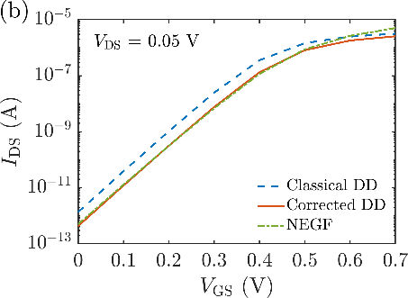
The KG solver implemented in NESS provides accurate electron mobility at low-field near-equilibrium conditions
[33,34]. It combines the quantum effects based on the 1D multi-subband scattering rates of the most relevant scattering mechanisms in confined channels
[19] and the semi-classical BTE by applying the KG formula within the relaxation time approximation
[11]. In the first step, the NEGF module of NESS is used to extract the electron densities, subband levels (
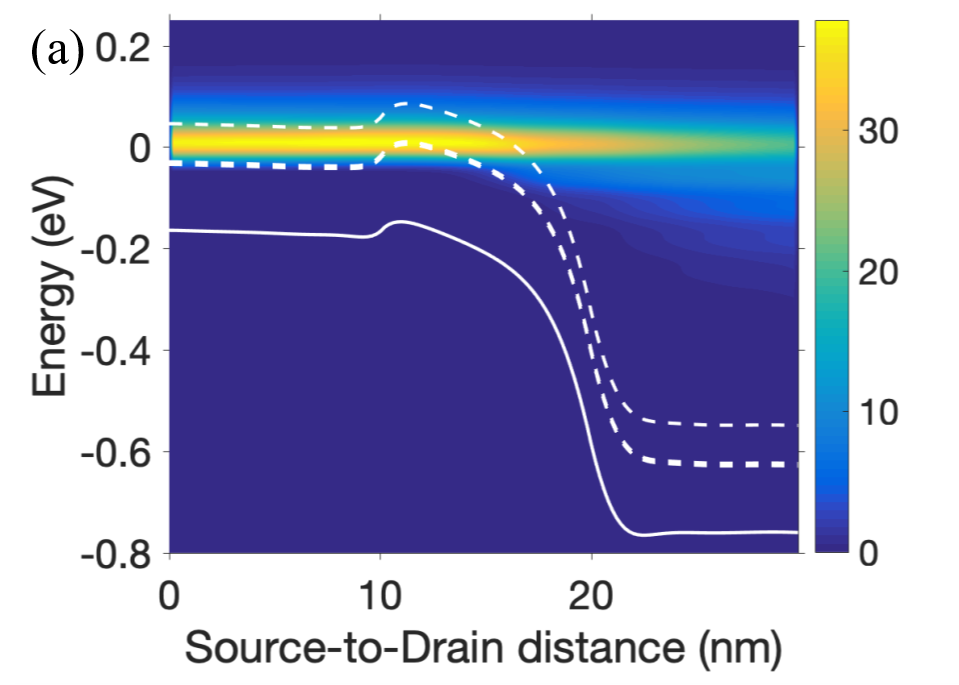
El ), and the corresponding wavefunctions (
ξl ) at the cross-section area of a gated NW in the presence of a low electric field in the transport direction (the long-channel device approximation).
In the second step, the 1D rates for the dominant scattering mechanisms in silicon are calculated using the parameters from the first step. The scattering rates are directly derived from the Fermi Golden Rule, using the time-dependent perturbation theory and assuming that the transitions between two states occur instantaneously. In this paper, we present two of the implemented scattering mechanisms:
Acoustic (Ac) phonon scattering is considered to be elastic and within the short-wave vector limit. Its equivalent equation from an initial subband l and a final subband l’ is:

(1)
where

is the acoustic deformation potential,

is the material density,

is the reduced Planck’s constant,

is the speed of sound,
ml is the electron effective mass in the transport direction,

are vectors normal to the transport direction,
θ represents the step function,

is the kinetic energy for a wavevector with magnitude
k,

is the energy separation between subbands
l and
l’, and

.
Optical (Op) phonon scattering takes into account g-type and f-type transitions (intra- and inter-valley transitions, respectively) and the energies of the different branches of the optical deformation potential are considered constant (as used in most of the standard approaches). Accordingly, the optical phonon scattering rate for the phonon mode j can be written as:

(2)
where

(3)
with

(4)
Here, nj is the phonon number, ωj is the phonon energy, DOp,j is the optical deformation potential, and mv (mv’ ) is the transport effective mass of the initial(final) valleys, respectively.
In the third step, the mobility (

) for the scattering mechanism
i and subband
l is calculated considering the semi-classical simulation of the transport properties of a 1D electron gas using the BTE within the relaxation time approximation
[11] as a function of the relaxation time (

), the 1D density of states (
gl ), the Fermi-Dirac function (
f0 ), and the 1D electron concentration (
Nl ):

(5)
In the fourth step, we calculate in two strategies the total mobility for the
l subband (
μl ):
(1) it is calculated as a function of the individual mobilities associated with each scattering mechanism (

) using the Matthiessen rule (

); and
(2) the scattering rates of all mechanisms are directly added to avoid the Matthiessen rule and thereby
μl is computed using Equation (5). The former strategy is of special interest for devices with large cross sections because the error induced by the Matthiessen rule in narrower devices is comparable to MS-MC and NEGF approaches. Finally, the average mobility of a NW structure is calculated accounting for all the subbands:

. The advantage of both semi-classical alternatives in comparison to purely quantum transport simulations is that the rates are individually computed and then combined, reducing dramatically the computational cost.
Table 1.
Main dimensions, doping values, and scattering parameters for the cylindrical Si NWs.
Device Parameters
| Si width | From 3nm to 6nm |
Scattering parameters | DAc | 14eV |
| SiO2 width | 0.8nm | DOp,j (g-type) | [5,8,30] ·109eV/m |
| Doping | 1015cm-2 | DOp,j (f-type) | [1.5,34,40] ·109eV/m |
| Temperature | 300 | ωj (g-type) | [0.01206,0.01853,0.063] eV |
| Effect. Mass | Ref. [1] | ωj (f-type) | [0.01896,0.0474,0.05903] eV |
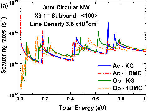
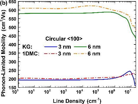
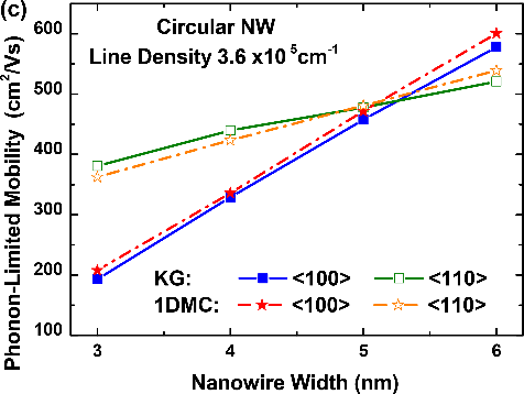
Figure 8.
Scattering rates and mobility comparison between the KG module from NESS and the 1DMC code from [10]: (a) Acoustic and optical phonon scattering rates of the first subband of valley X3 as a function of the total energy for a 3nm circular NW with a line density of 3.6×105cm-1 and ⟨100⟩ orientation. (b) Phonon-limited electron mobility as a function of the line density for 3nm and 6nm circular NWs with ⟨100⟩ orientation. (c) Phonon-limited electron mobility as a function of the width for circular NWs with a line density of 3.6×105cm-1, ⟨100⟩ and ⟨110⟩ orientations. Figure 8 shows the scattering rates and mobility for cylindrical Si NWs, which main parameters are summarized in Table 1. The results from the KG module have been compared to the results of an external to NESS 1DMC simulator
[10], where the mobility is extracted after applying a small constant electric field by fitting the average velocity versus field dependence. In general, the 1DMC and KG scattering rates for the lowest subband of the 3nm nanowire (Figure 8(a)) are in very good agreement especially at low energy levels, the most relevant region which determines the accuracy of the low-field mobility calculations. Moreover, the phonon-limited mobility computed with both approaches shows a very good agreement as a function of the line density (Figure 8(b)) for a 3nm and 6nm circular NW with ⟨100⟩, and as a function of the NW widths (Figure 8(c)) at a fixed line density for ⟨100⟩ and ⟨110⟩ orientations.