Research Article Current Issue Versions 2 Vol 4 (2) : 21040201 2021
Download
Improvement of Environment Stability of an i-Line Chemically Amplified Photoresist
1367 35 0
Abstract & Keywords
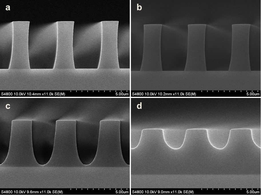
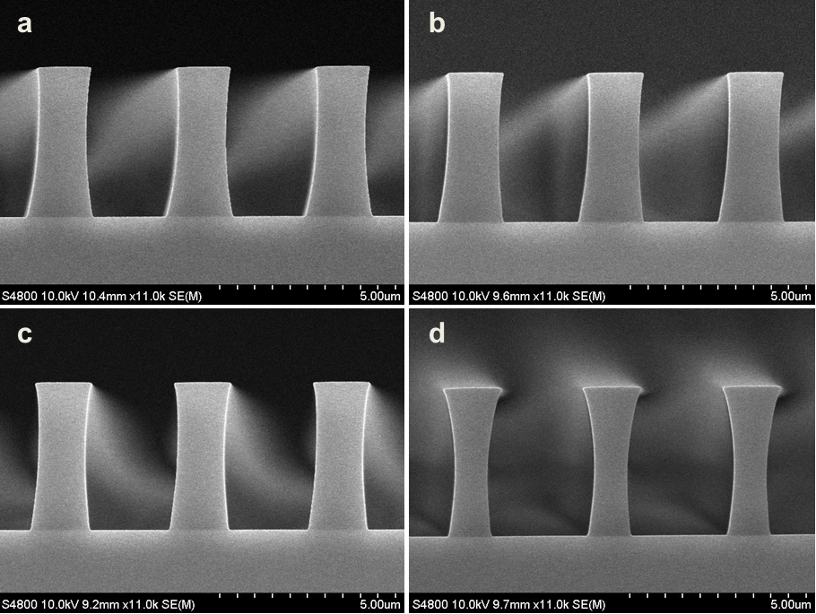
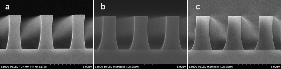
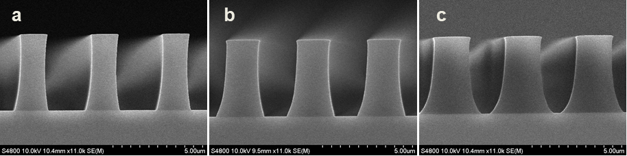
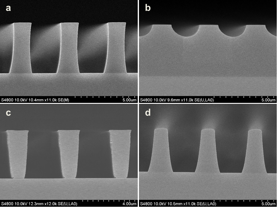
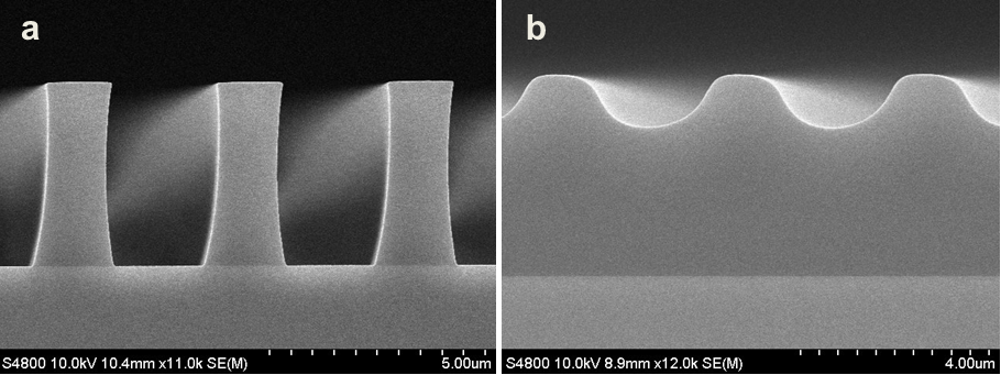
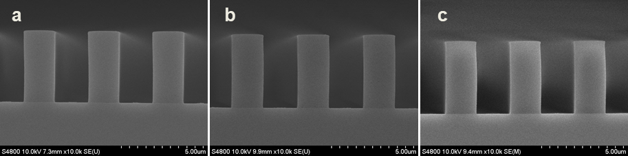
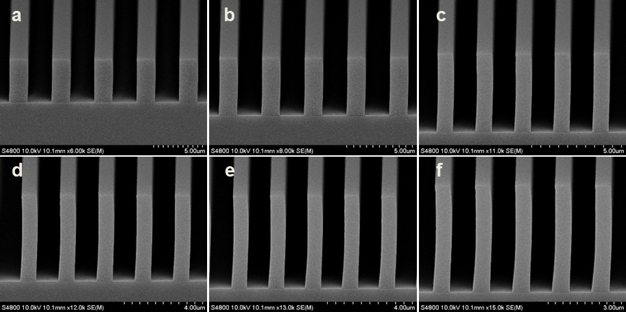
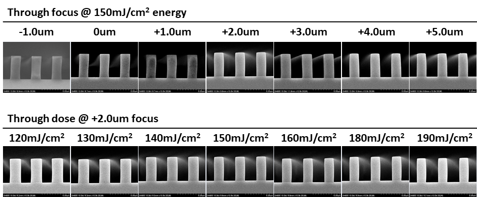
Abstract: An i-Line chemically amplified (ICA) thick film positive resist is reported in this paper. The impact of process conditions on photoresist performance was investigated. Pre-apply bake temperature and post exposure bake temperature affect acid diffusion and deblocking reactions, thus playing an integral role in defining the resist profile. Both pre-apply bake delay and post exposure delay (PED) affect critical dimension (CD) variation, but PED is more sensitive to contact with airborne contaminants. Different polymers and different photo-acid generators (PAG) are also illustrated in this work. By optimizing the structure and concentration of key components, an ICA resist with good environment stability and excellent lithographic performance was demonstrated.
Keywords: Chemical amplification; thick film; i-Line; environment stability; Poly (p-hydroxyl styrene); PAB; PEB
1.   Introduction
Modern demands for semiconductor manufacturing has pushed requirements and process technologies for traditional materials into more advanced nodes. Thick film resists were commonplace in advanced semiconductor manufacturing in layers such as passivation, PAD, and thick implant processes. Conventional Novolak/DNQ type i-Line positive resists were widely used in such applications. They have many benefits such as cost efficiency and reliability because they are mature processes. But as film thickness increases, Novolak/DNQ type resists suffers drawbacks such as, substantial long re-hydration time for photo chemistry reaction, sloped profile, and slow photospeed due to the high absorption of Novolak resin. Photoreaction of DNQ generated N2 can also generate bubble defects [1 ].
To solve these drawbacks, chemical amplification (CA) technology was introduced to i-Line lithography. Chemical amplification in lithography was first applied in KrF resist. Blocked Poly (4-hydroxyl styrene) was adopted to overcome the high absorbance of Novolak at 248nm. And the deblocking reaction catalyzed by H+ generated from onium salts provides fast photospeed [2 ,3 ].
During initial KrF CA resist development, scientists found that KrF CA resists are easily affected by airborne base contamination. These bases could diffuse into the resist film, neutralizing the acid generated during exposure. This “poisoning phenomenon” is referred to as T-top defect [4]. To solve this problem, high activation energy (Ea) resists and low Ea resists were developed. High Ea platforms often use high bake temperatures, which can densify the resist film and reduce the diffusion of airborne base [5]; while low Ea platforms can react at room temperature, which can reduce the impact of diffused base contaminates [6]. Another approach is to use base as an additive to desensitize the resist to base contaminants [7]. Along with formulation optimization, both global chemical filters (clean room) and local chemical filters (inside scanner and track) were used to reduce the base contamination of the environment [8].
Compared with KrF fabs, i-Line fab cleanrooms did not consider global or local base control, which limited the application of ICA resists. In this paper, the effects of bake processes and delay time before and after exposure are investigated. The influences of different polymers and PAGs on resist performance are also discussed.
2.   Experiment
2.1.   Tools
Nikon I9c i-Line stepper (NA 0.58, Sigma 0.6) is a widely used in 6’’ wafer IC manufacture. Mark V from TEL is an automatic track for resist spin-coating, baking and development processes. The thickness of photoresist film thickness was measured by F50 from Filmetrics. CD-SEM S8840 from Hitachi is used to measure top-down CD of features. Hitachi S4800 was used for cross-section profiles observation. UV-Vis spectrophotometer from Labtech was used for UV absorbance of polymer at 365nm wavelength.
2.2.   Chemicals
Poly (4-hydroxyl styrene-co-t-butyl-acrylate) (PHS-PtBA)
Poly (4-hydroxyl styrene-co-styrene-co-t-butyl-acrylate) (PHS-PS-PtBA)
Ethyl vinyl ether blocked PHS (EVE-PHS)
Ethyl vinyl ether blocked novolak (EVE-novolak)
PAG-1(triflic acid generator)
PAG-2(toluene sulfonic acid)
PAG-3(hydrochloric acid)
Propylene glycol monomethyl ether acetate (PGMEA)
Acetonitrile
2.3 Lithography Process
The ICA resist was prepared by adding polymer, PAG, base, and additives into PGMEA. Then the mixed solution went through a 0.2um PTFE filter. After spin-coating on a Si wafer, the 4.2um thick resist process conditions were as follows: pre-apply bake (PAB) at 100~130 ℃ for 180s, exposure on Nikon I9c i-Line stepper, post-exposure bake (PEB) at 90 ℃ for 60s, and then development in a 0.26N TMAH aqueous solution for 60s. The target feature size was 2um L/S.
The CD was measured by Hitachi CD-SEM S8840. For each wafer, 9 points were measured and the average CD and standard deviation are reported in this work.
The profiles of features were obtained using an Hitachi X-SEM S4800.
The absorbance of polymers was determined by UV-Vis spectrophotometer. The PHS type polymers were dissolved in acetonitrile at 10wt%, and the EVE-Novolak was dissolved in acetonitrile at 0.1wt%. Then UV absorbance at 365nm of both solutions was measured and normalized to 10wt% concentration.
3.   Results and Discussion
3.1.   Bake Temperature Impact
An ICA resist with the high Ea polymer, PHS-PtBA, and triflate PAG-1 was evaluated with a bake temperature matrix using 150mJ/cm2 exposure dose. First PEB was set at 90 ℃ and PAB temperature varied from 100 ℃ to 130 ℃. From Table 1, we can see that CD increased as PAB temperature increased. This was caused by a denser film at higher PAB temperature, which limited the diffusion of acid and gave a small reaction diffusion length. The dense film made it difficult for the developer to penetrate the resist. As shown in Figure 1, at 130 ℃ PAB, the space could not open at the same exposure dose.
Table 1.   CD change of ICA resist with different PAB temperature.
PAB (℃)100110120130
Feature size (um)2.0652.1243.328Not open
STDEV. (um)0.05030.05180.1954


Figure 1.   Profiles of ICA resist with different PAB temperature: (a) PAB at 100℃; (b) PAB at 110℃; (c) PAB at 120℃; (d) PAB at 130℃.
Then PAB temperature was set at 110 ℃, and PEB temperature varied from 90 ℃ to 120 ℃. As shown in Table 2, CD measured by CD SEM shows a slight decrease as PEB temperature increases. This is because high PEB temperature gives faster deblocking reactions and thus smaller CD. As shown in Figure 2, with the increase of PEB temperature, the bottom CDs were getting smaller, while the top CDs didn’t change much. The shape turned into a reverse trapezoid when the PEB temperature rose above 120 ℃. Formation of the reversed trapezoid pattern is complicated. It involves acid distribution during exposure, acid redistribution during PEB and the deblocking reaction during PEB. For the formulation that is shown, triflic acid was generated during exposure. Its small size and strong acidity make it easy to diffuse within the resist film and easy to evaporate from the top of the resist to the environment. At low PEB temperatures, there was a mild evaporation of acid from the top of the film, and diffusion within the film and the deblocking reaction had similar rates, so that the total results of diffusion and reaction was a vertical sidewall. But at high PEB temperature, there was more evaporation of acid from the top of the film, and, since the reaction was faster, the acid diffusion length was smaller, thus the total results of diffusion and reaction formed a reverse trapezoid pattern. To get a more vertical profile, the polymer/PAG interaction needs to be fine-tuned during exposure and PEB.
Table 2.   CD change of ICA resist with different PEB temperature.
PAB (℃)90100110120
Feature size (um)2.0651.9571.9991.946
STDEV. (um)0.0500.0320.0470.043


Figure 2.   Profiles of ICA resist with different PEB temperature: (a) PEB at 90℃; (b) PEB at 100℃; (c) PEB at 110℃; (d) PEB at 120℃.
3.2.   Pre-exposure Delay and Post-exposure Delay
Delay between different lithography processes is common in IC fabs, especially during troubleshooting or equipment maintenance. ICA resist is sensitive to environmental contaminates, such as base and acid. In this section, two types of process delay, delay between PAB and exposure, and delay between exposure and PEB were evaluated. For the first type of delay, the wafers with resist films were not exposed right after the PAB process, but preserved in the clean room without airborne contamination control for 1h and 2h. Then the wafers went through the rest of the lithography processes and formed patterns after development. The top-down CD increased by 12.9% to 2.332um for a 1h delay, and by 19.4% to 2.466um (Table 3) for a 2h delay. This indicated that the resist film absorbed airborne amine during the delay time. The amine neutralizes H+ generated during exposure, which hinders the reaction between H+ and blocked PHS. The longer the delay time, the larger the CD as outlined below (Figure 3).
Table 3.   CD change of ICA resist with different pre-exposure delay time.
Pre-exposure delay (h)012
Feature size (um)2.0652.3332.466
STDEV. (um)0.0500.0930.080


Figure 3.   Profiles of ICA resist with different pre-exposure delay time: (a) no delay; (b) delay for 1h; (c) delay for 2h.
For the second type of delay, wafers with resist were delayed between exposure and PEB. The wafer was kept in the clean room for 1h and 2h, then went through the rest of the lithographic process. Compared to pre-exposure delay, post-exposure delay had more influence on feature size. The top-down CD increased by 28% to 2.644um for a 1h delay, and by 60% to 3.305um (Table 4) for a 2h delay. In post-exposure delay, the H+ directly reacts with airborne amine. The CD and profiles increased and small T-top structures were observed at the tops of patterns (Figure 4).
Table 4.   CD change of ICA resist with different post-exposure delay time.
Post-exposure delay (h)012
Feature size (um)2.0652.6443.305
STDEV. (um)0.0500.1640.200


Figure 4.   Profiles of ICA resist with different post-exposure delay time: (a) no delay; (b) delay for 1h; (c) delay for 2h.
3.3.   Polymer Impact on Profiles
To optimize the overall performance of ICA photoresist, several different types of blocked polymer were investigated, such as PHS-PS-PtBA, EVE-PHS and EVE-novolak. Compared to PHS-PtBA, High Ea polymer PHS-PS-PtBA was harder to deblock by H+ catalysis; and even after full deblocking, there were fewer -COOH groups generated, thus giving a small Rmax, so it was not suitable for a thick film application. Shallow trenches were formed in resist film even the exposure dose was raised to 1000mJ/cm2. On the other hand, Low Ea polymer EVE-PHS polymer formed patterns at exposure doses under 30mJ/cm2. Severe undercuts and standing waves were observed along with the trapezoid sidewalls. This can be explained in the following mechanisms:
1) EVE-PHS is more transparent than EVE-novolak at 365nm, which gives a relatively high exposure dose at the bottom of the resist film;
2) The substrate used is bare silicon, which has strong reflection of 365nm wavelength. Combined with the high exposure dose at the bottom, this gives a reversed trapezoid pattern;
3) EVE-PHS can easily deblock when acid is present, even at room temperature, thus the acid generated during exposure does not have enough time to diffuse, which induces strong standing waves.
Meanwhile, the low Ea polymer EVE-novolak showed tapered profiles due to the high absorbance of novolak at 365nm (Figure 5).
Table 5.   The absorbance of different polymer in acetonitrile at 365nm.
PolymerPHS-PtBAPHS-PS-PtBAEVE-PHSEVE-novolak
Absorbance0.3630.66040.0234.577


Figure 5.   Profiles of ICA resists with different polymers: (a) PHS-PtBA; (b) PHS-PS-PtBA; (c) EVE-PHS; (d) EVE-novolak.
3.4.   PAG Impact
CA resist uses H+ generated from PAG during exposure to catalyze deblocking reactions of polymers. The PAG is critical for resist lithography performance. Three different types of PAGs were evaluated in the high Ea PHS-PtBA platform. The anion type affects the strength and diffusion length of H+, which will affect the photospeed and profile of resists. PAG-1 generates triflic acid with strong acidity and long diffusion length. Periodic Line/Space patterns were obtained with catalysis of triflate acid under 150mJ/cm2 exposure dose. The acidity of toluene sulfonic acid from PAG-2 is weaker than triflic acid. Shallow trenches were observed at the surface of resist with PAG-2, even though the exposure dose was raised to 1200 mJ/cm2 (Figure 6). The hydrochloric acid from PAG-3 is the weakest acid and it hardly catalyzed the deblocking reaction. There was no pattern formed in the resist with PAG-3.


Figure 6.   Profiles of ICA resists with different PAGs: (a) PAG-1triflic acid generator; (b) PAG-2 toluene sulfonic acid generator.
3.5.   Demonstrate Photoresist Performance
By optimizing the polymer structures and PAG/base choices, an environmentally stable ICA resist was developed by Kempur. C9005 has dramatic airborne amine resistance. It could maintain a stable CD uniformity after 2h pre-/post- exposure delay (Table 7). The rectangular profiles of C9005 were barely changed after 2h delay (Figure 7).
Table7. CD change of ICA resist with different pre-/post –exposure delay.
 
No delayPre-exposure delayPost-exposure delay
Delay time(h)01212
Feature size (um)2.0082.0522.0792.0642.112
STDEV. (um)0.0500.0480.0690.0660.058


Figure 7.   Profiles of ICA C9005 with delay: (a) No delay; (b) Pre-exposure delay for 2h; (c) Post-exposure delay for 2h.
Due to high transparency of polymer used, C9005 showed a good resolution (Figure 8). We obtained 0.75um L/S features in 4.2um resist thickness. The aspect ratio reached 5.6.


Figure 8.   Resolution of C9005 at 4.2um thickness: (a) 2um L/S; (b) 1.5um L/S; (c) 1um L/S; (d) 0.9um L/S; (e) 0.8um L/S; (f) 0.75um L/S.
C9005 has a broad process window (Figure 9). It can achieve 6um of depth of focus and 46.7% of exposure latitude for +/- 10% of CD variation. It can be utilized for different layers and applications.


Figure 9.   Process window of C9005 at 4.2um thickness.
4.   Conclusion
By tuning process conditions and formulation, a high resolution I line chemical amplified photoresist with good environmental stability was developed. Some learnings from the development process are shared in this paper.
[1] P. M. Dentinger, K. L. Krafcik, K. L. Simison, R. P. Janek, J. Hachman, High aspect ratio patterning with a proximity ultraviolet source. Microelectronic Engineering61-62 , 1001-1007 (2002).
[2] E. Reichmanis, F. M. Houlihan, O. Nalamasu, T. X. Neenan, Chemically amplified resists: Chemistry and processes. Advanced Materials for Optics and Electronics4 , 83-93 (1994).
[3] J. Crivello, Applications of photoinitiated cationic polymerization to the development of new photoresists. (1984).
[4] S. MacDonald et al., Airborne chemical contamination of a chemically amplified resist. Microlithography (SPIE, 1991), vol. 1466.
[5] W. Conley et al., in Advances in Resist Technology and Processing XIII. (International Society for Optics and Photonics, 1996), vol. 2724, pp. 34-60.
[6] S. Malik et al., Polymer Structural Variation Towards Enhancing KrF Resist Lithographic Properties. Journal of Photopolymer Science and Technology11 , 431-438 (1998).
[7] T. B. Michaelson et al., in Advances in Resist Technology and Processing XXI. (International Society for Optics and Photonics, 2004), vol. 5376, pp. 1282-1293.
[8] J. Maltabes et al., 1X deep-UV lithography with chemical amplification for 1-micron DRAM production. Microlithography '90 (SPIE, 1990), vol. 1262.
Article and author information
Haibo Li
Qian Yang
Jia Sun
Jie Li
Meng Guo
Bing Li
Publication records
Published: None (Versions2
References
Journal of Microelectronic Manufacturing