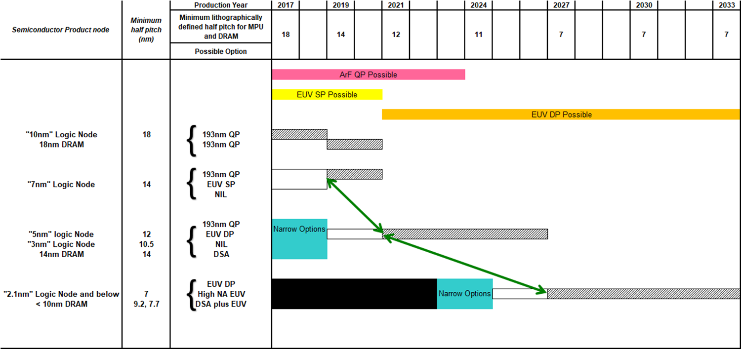
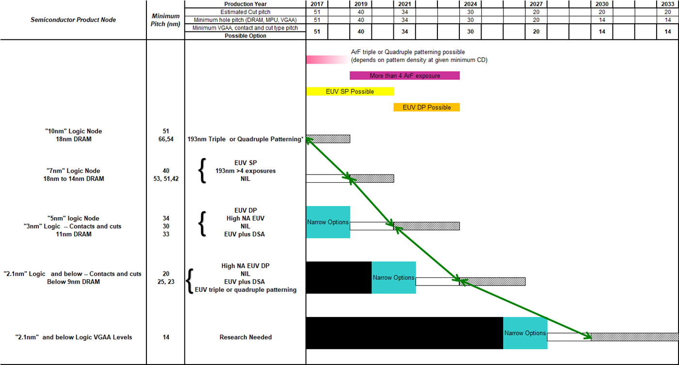
Figure 1 shows the patterning requirements table of the 2017 roadmap. It is separated into sections for DRAMs, flash memory and high-performance logic chips. The cells are color coded. White means that the manufacturing technology exists that can meet the requirement, yellow means that technology that can meet the requirement is known, but not implemented in manufacturing, and red indicates that technology needs to be developed. DRAMs will need new technology for better resolution in 2024 and logic will need new technology for better resolution in 2021. The needs of high-performance logic chips is thus the driver for improved patterning resolution in the semiconductor industry. Memory technology is the driver for lower cost patterning methods. Flash memory used to drive lithography technology, but the industry turned to 3D flash which stacks memory cells on top of each other to enable higher bit densities instead of continuing to shrink cell sizes. 3D flash memory has many challenges of its own, especially in etch and deposition, but shrinking critical dimensions is not one of them. Thus all the cells in the requirements table for flash memory are white.
In the past, simple shrinks of critical dimensions for CMOS logic devices gave improved performance. Improvements in patterning technology directly gave improved devices. However, as device dimensions got smaller and smaller, electrical factors such as current leakage forced innovation in device design. In 2005, the rate of gate length change for logic device slowed down even though the rate of growth in devices per area of silicon did not slow down
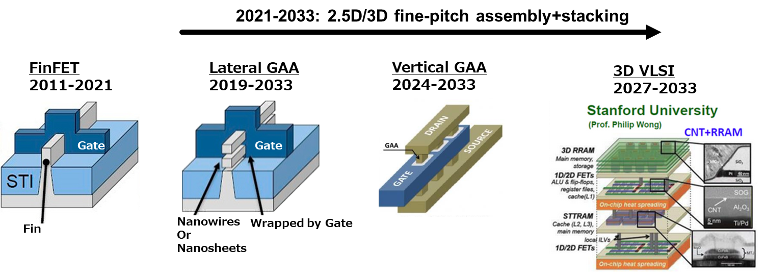
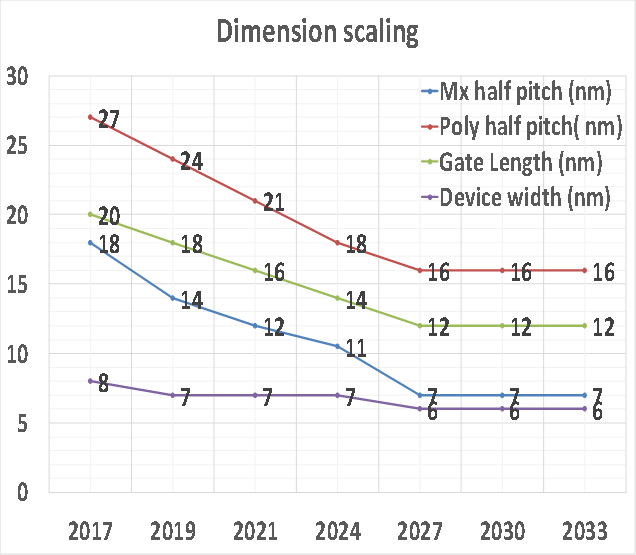
[2]. This was the result of device design innovations. In 2011, the FinFET was introduced to manufacturing, where the gate was redesigned into a vertical structure to improve leakage performance and give better performance. The requirement for device innovation at the same time as reduction in critical dimensions to give improved chip performance will continue. Figure 2 shows projected device structures from the More Moore Roadmap. FinFETs are expected to be replace by lateral gate all around structures (LGAA), then by vertical gate all around structures (VGAA), which will then scale in 3D instead of shrinking further. It is important to note that these design innovations are required in the future for the semiconductor needs of its target customers. Without introducing new types of devices, the industry will not able to provide the chip performance needed in the future. Projected key dimensions of logic chips over time are shown in Figure 3
[3]. Once 3D structures are introduced then horizontal scaling will stop. Thus, we can consider the short-term future to be the next seven to ten years where new logic device types are introduced simultaneously with shrinking critical dimensions and the long-term being 10 years or more from now where high-performance logic devices have switched to vertical scaling in order to increase device density in logic chips.
Figure 1.
The 2107 IRDS Roadmap Patterning requirements. Figure 2.
Projected structures for high performance logic devices. Figure 3.
Projected critical dimensions for high performance logic devices. 3. The State of Current Patterning and Possible Future Patterning Options
Multiple patterning using ArF immersion lithography is in use for all advanced chip designs today. Pattern multiplication has been qualified and in production since at least 2017. The resolution capabilities of multiple patterning are excellent, and resolution could be smaller than it is today, especially if more than four litho etch steps were used. However, shrinking features further or going beyond quadruple patterning creates difficult challenges in tolerance and overlay control and results in a process where the development time for the shrinking of for a new chip design is unacceptably long. Semiconductor makers want alternatives. The four new types of patterning under substantial development today and considered in this roadmap are directed self-assembly (DSA), nano-imprint (NIL), direct write ebeam lithography (maskless lithography or ML), and extreme ultraviolet lithography (EUV).
DSA is a technique that uses special polymers that separate into microphases when annealed. Guide structures are formed using lithography and the guide structures “direct” the polymer to separate into phases in usable arrangements during anneal, for example parallel vertical lamellae or vertical cylinders. The resulting pattern of phases is “developed” through etching to give the desired pattern. A cut level or other level is used to restrict the lines and spaces or the holes to the areas of the chip where they are desired. It promises to be inexpensive and to have high resolution. The first systems and processes used poly(styrene)-b-poly(methylmethacrylate) as the polymer and had a line and space minimum resolution of about 12nm to 13nm
[4]. DRAM companies evaluated it, but in 2015 Micron reported that DSA did not give the same pattern quality for lines and spaces that their high-volume manufacturing technique, presumably multiple patterning did
[5]. Process flows for other types of circuit patterns have been reported since then
[6], but no successful implementation has occurred. Key issues are defects, pattern overlay and inspection. Defects are particularly hard to find, because they can be at the bottom of three-dimensional structure composed of different polymer phases where only the top of the structure is accessible to inspection before etch. Work on DSA materials that can achieve smaller dimensions has continued, and this work holds out hope for the future.
NIL involves creating a template with patterned grooves where lines will be and small pillars where contact holes will be. A master template is used to make secondary templates and the secondary templates are used to stamp a pattern into “resist” that has been applied to the wafer through an ink jet sort of printing process. The templates are transparent and UV light is used to cure the resist with the template still in place. Then the template is peeled away, leaving a relief pattern in the resist
[7]. Because it is a method of contact printing the patterning can be affected by the accumulation of defects and this is why a system of disposable secondary templates is used. The templates are 1X, meaning that they are the same size as the patterns they print, unlike typical optical reticles. However, it promises low cost and has made great progress in achieving the performance needed for production of 3D NAND flash memory. Production tools are available and currently being qualified for potential use in memory production in 2019.
Direct Write Ebeam lithography uses focused beam of electrons to expose a resist in a pattern created by magnetically deflecting the beam to different locations. The resulting pattern is a function of software and doesn’t use a mask for pattern generation. If one electron beam is used the technique is suitable for slowly creating small numbers of circuits for research purposes but does not have the throughput to meet the needs of any volume chip maker. Massively parallel ebeam writing is needed to get a usable throughput for actual volume semiconductor production. Producing tools that can do this at the required dimensions has proved a big challenge. Work was reported on this technique for chip making in 2015
[8], but then apparent progress stopped. Developing a reliable small generator of many e-beams was difficult and delayed the program. But in 2018, the Mapper tool, FLX-1200 was described, which uses 65,000 parallel electron beams. It was operational and produced 42nm half pitch lines with a measured throughput of about 4 hours per wafer. A roadmap to a throughput of about one and a half hours per wafer was described
[9]. While this dimension may seem large compared to the dimensions in Figure 1, and the throughput slow, it is still of interest to chip makers. If successful, it will enable cost effective production of very chip designs with very low production volumes and also enable the personalization of chips so that every chip on wafer has a unique ID.
EUV lithography is like traditional optical lithography in that light is projected on a wafer from a patterned mask and involves a mask that is four times larger than the printed pattern. The resolution is much better than that of ArF immersion and this could enable single exposures that replace multiple ArF immersion exposures. It reduces both development and manufacturing cycle time for semiconductor makers. It can also reduce cost if the productivity of the EUV tool is high enough. It is particularly cost effective for chip designs that have limited production, because the cost of the mask set per chip made is particularly high for such designs.
The EUV wavelength is so short that all the optics, including the mask, are reflective and the system operates in a high vacuum. Each mirror involved in the optical train has about 65% reflectance, that is, is absorbs 35% of the light. There are typically 6 mirrors in the lens, plus more in the illuminator and there is the mask also, the fraction of the light source that actually reaches the mask is something like 0.65 raised to the tenth power. This loss of power in the optical train puts a tremendous stress on the illumination source power. The lack of sufficiently powerful light sources limited throughput and held EUV back from production for a long time. After many years of development, ASML reported in 2018 that EUV exposure tools with 250 watts of power at intermediate focus were shipping in 2018
[10]. They reported that this power would enable a manufacturing level of throughput of 125 wafers per hour assuming a resist exposure dose of 20mJ/cm
2. Although no production resist can provide sufficient quality imaging at this dose, resists are available that image at somewhat higher doses, and this is still enough power that both Samsung and TSMC have announced 7nm node logic process that will go into production in 2019. Challenges for EUV include defectivity, mask blank supply, pellicle development, line edge roughness, line width roughness and critical dimension uniformity.
A special mention about stochastics is needed. Stochastics refers to random effects due to the natural variations in the number of photons, the positions of key reactions in resist and the randomness of the actual placement of materials when looked at on a molecular scale. Stochastics are responsible for creating line edge and line width roughness and are responsible for some of the random critical dimension and positional variations of critical features in leading edge processes. As feature sizes shrink, stochastic effects do not shrink in magnitude. Instead they become a larger proportion of the error and tolerance budgets for critical dimensions. In ArF lithography, stochastics are responsible for line edge and line width roughness. In EUV, significant stochastic effects are driven not only be the random variations in resist chemistry, but also by random variations in the actual exposure dose due to the quantum nature of light. The number of photons in an EUV exposure is fourteen times smaller than the number of photons in a comparable ArF exposure. It is small enough that shot noise effects are a real issue for EUV, and an issue that will get worse as feature sizes continue to shrink. Stochastics can cause actual killer defects, not just critical dimension variations and feature roughness. Unfortunately, the number of opens and shorts and closed contact holes due to stochastic variations are larger (that is, worse in frequency) than one would predict from simple calculations assuming a normal distribution of critical dimensions with a given mean and sigma. This has been shown both by detailed simulation
[11] and by experiment
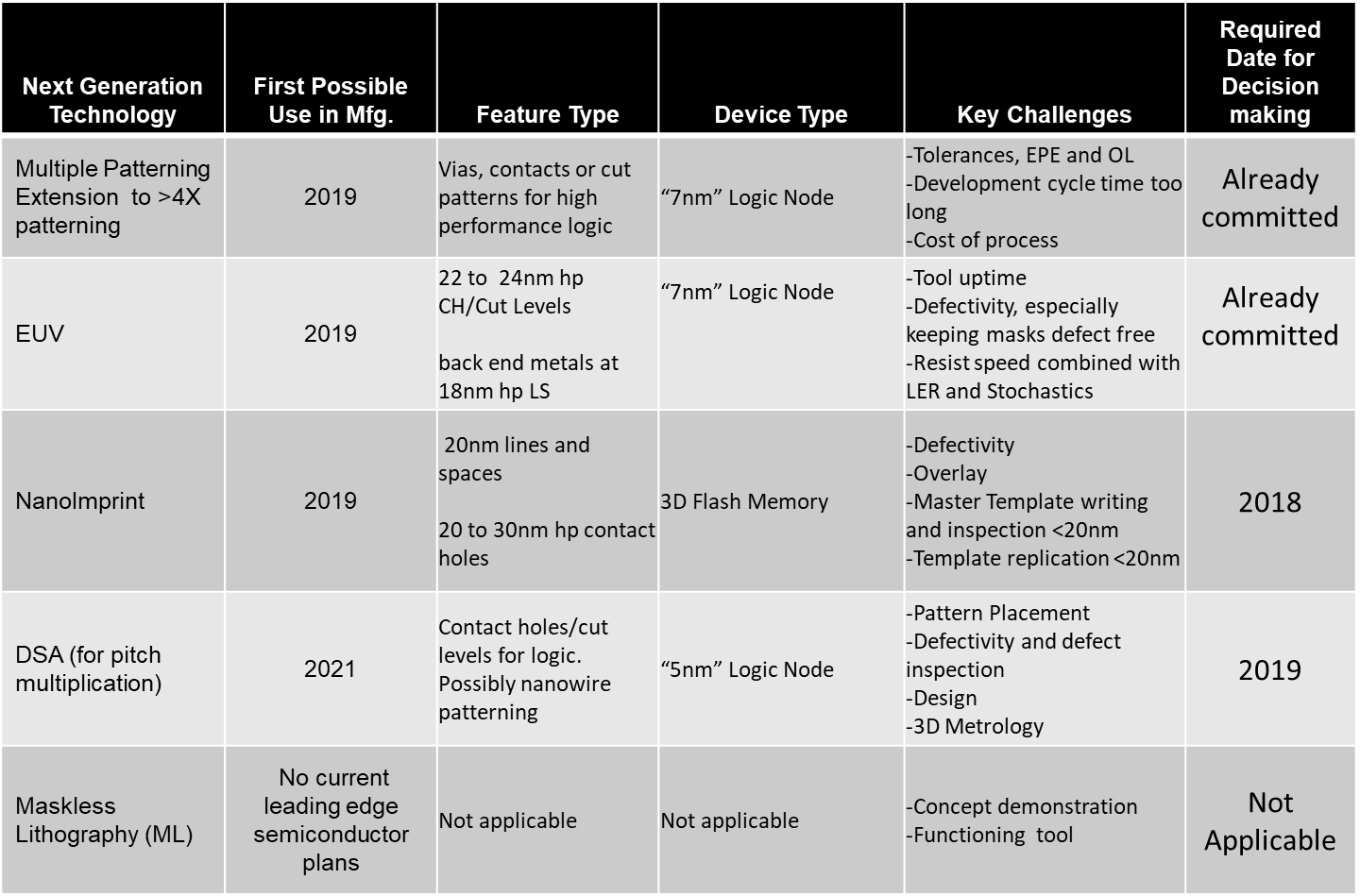
[12]. The extension of EUV to smaller feature sizes will be challenged more by the need to control stochastic effects than by anything else. Table 1 summarizes the status and challenges for each of the technologies discussed above.
Table 1.
Difficult challenges for each patterning technology.