Research Article Archive Versions 2 Vol 2 (2) : 19020203 2019
Download
Patterning Defect Study for Process Integration Engineering Using Pattern Fidelity Monitoring with Review SEM Images
: 2019 - 05 - 24
: 2019 - 06 - 28
2124 45 0
Abstract & Keywords
Abstract: Normally the optical wafer inspection tools are used for advanced process control in high volume manufacturing of semiconductor devices. The SEM Review is done for limited sample of inspection defects to do defect based process characterization. The defect classes that are monitored normally indicate process and random defect issues. There is limited to no information of patterning related issues in real time defect monitor. Moreover, with the objective of process integration engineering of multiple processes it becomes harder to see the evolution of a defect in the line. The Die-to-Database Pattern Monitor (D2DB-PM) solution has addressed this problem. It uses the existing high resolution images from the Review and Metrology tools and compares the pattern shapes with the design reference. This way it captures patterning deviations in real time. Here we report the subtle defect problem encountered in process integration and the results from using the D2DB-PM solution. We found that this approach reduces the workload on CDSEM tools by analyzing SEM Review images instead and the automated reports improves the efficiency of all process teams.
Keywords: Die-to-database Pattern Monitor; After Develop Inspection (ADI); After Etch Inspection (AEI); SEM Review; CDSEM; pattern centric; pattern monitor
1.   Introduction
The standard semiconductor wafer fabrication process starts with photolithography where the pattern transfer is done from the reticle to the photoresist layer on the wafer. Rigorous patterning control is achieved with Resolution Enhancement Techniques (RET) that are applied to the original design to ensure that the pattern printed on the wafer is as close as possible to the design intent. The arduous Optical Proximity Correction (OPC) verification and hotspot management is done to spot any shortcoming and fix it before further wafer material processing [1-3]. Finally, the process control at critical wafer process steps is done to ensure integrity of the semiconductor manufacturing process. At times, still with the entire existing process control infrastructure, we run into patterning defect issues [4]. Here we report an innovative methodology of Pattern Monitor that complements existing process control techniques and consistently detects critical pattern defects on wafer that are hard to find using conventional wafer inspection tools. The unique integrated pattern centric approach makes this method unique among current inline process control methodologies.
In the conventional method, different metrology and inspection tools are used to perform measurement and defect inspection. A predetermined list of critical design locations from post OPC verification is fed to a Critical Dimension Scanning Electron Microscope (CDSEM) tool to collect critical dimension and high resolution image data from the wafer. A full wafer scan is subsequently performed with an optical inspection tool, and that is followed by high resolution image capture at a limited number of sampled locations to determine the defectivity and complexity of this exacerbates with smaller design features [5]. Both these metrology and inspection steps require significant time for tool recipe preparation and present a throughput bottleneck. In the case of critical wafer monitoring steps such as Process Window Qualification (PWQ), the turnaround time is relatively longer because of the necessity of collecting more information from the wafer. The results from this work have been presented before [6]. Previous studies have reported basic integration of image-to-design methodologies [7, 8].
The comparison of the conventional Process Window analysis with CDSEM tool data with the new efficient D2DB-PM method is shown in Figures 1 and 2.


Figure 1.   Conventional process window analysis.


Figure 2.   Efficient D2DB-PM method for PW analysis.
2.   Die-to-Database Pattern Monitor Solution
The D2DB-PM solution from Anchor Semiconductor processes high resolution images and performs shape and critical dimension analysis of the patterns. It utilizes already existing Scanning Electron Microscope (SEM) Review images from inline tools to perform Die-to-Database pattern shape and critical dimension evaluation and detect deviations inline, as shown in Figure 3. A pattern centric engine is the key to this solution that is used to process large volumes of SEM images rapidly as shown in Figure 4. This helps to resolve the measurement bottleneck that is otherwise associated with CDSEM tools.


Figure 3.   Data flow for pattern centric D2DB-PM solution.


Figure 4.   Schematic for pattern analysis [9].
The full chip design layout is deconstructed into critical patterns and is used to align with the features obtained from the SEM images. Computational techniques are employed to compare the data obtained from the wafer with corresponding reference layout patterns. All the relevant data associated with a particular pattern are saved in a Database. This solution tracks the subtle variations in the patterns that are captured from SEM images. It can track the behavior of all the individual patterns, thereby providing a means to determine weak and strong patterns in the full chip design [9, 10]. Because this approach relies on real wafer data, it creates a parallel baseline for process monitoring. Additionally, the effects of defect location accuracy errors from the optical inspection tools are minimized or eliminated by the D2DB-PM solution because it aligns every image to the reference design. Therefore the corrected location coordinates can be used for subsequent high precision root cause analysis such as marking precise locations for failure analysis.
3.   Case Study Results and Discussions
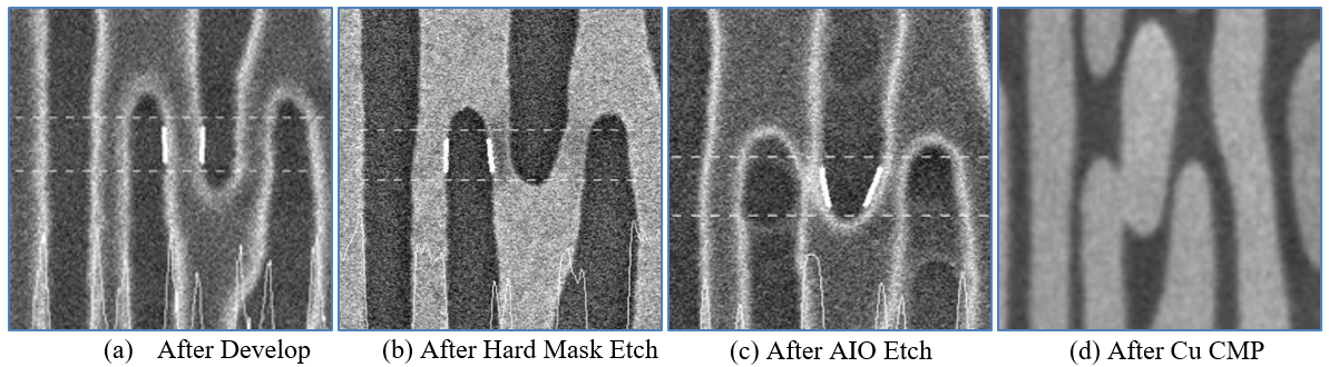
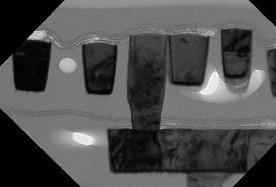
Here we will share results from the study of a 28nm device covering multiple process layers. In the case under consideration here, bridging defects were observed in the M1 process layer and were detected only after Metal Chemical-Mechanical-Planarization (Cu-CMP) process step, as shown in Figure 5(d). The conventional optical wafer inspection was set at the standard process control steps: After Develop  After Hard Mask Etch  After All-in-One Etch  After Cu CMP, but it failed to detect any anomaly in patterning at the preceding steps. The cross-section Transmission Electron Microscopy (TEM) analysis also confirmed the bridging of the adjacent M1 lines, as shown in Figure 6. Subsequent trace back analysis by defect location, as shown in Figure 5, revealed that the pattern deformation was not sufficient at the preceding process control steps to trigger optical defect detection with Die-to-Die wafer inspection. This is a fundamental weakness of the conventional wafer inspection and review methodology.


Figure 5.   Critical defect - subtle progression through process steps.


Figure 6.   
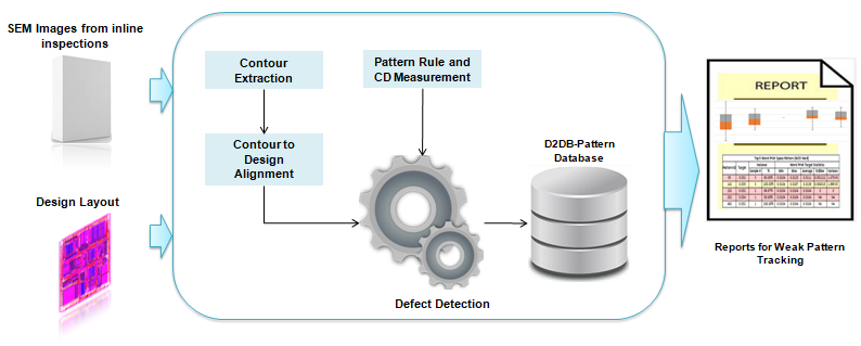
A critical defect - Cross TEM analysis of failed sample.
In addition to the need to improve defect detection there was a requirement for expanding the sample size for the measurement of critical dimensions for determining a more accurate process window. So it was decided to apply the D2DB-PM solution to perform root cause study from the lithography step to the final metal fill and CMP process steps using a process window qualification (PWQ) wafer. The potential to run fully automated analysis of SEM Review images offered an opportunity to collect a huge volume of images from the wafer– which is otherwise impractical to do on a CDSEM platform. With a combination of inputs from OPC verification results and the PWQ optical wafer inspection, a set of about 200 die locations were shortlisted for SEM review across and beyond the process window die. The data flow outlined in Figure 3 was employed by the team for automatically processing the thousands of SEM images that were collected after every process step. The automated D2DB-PM solution measured the feature size of all patterns-of-interest falling within the field of view of every SEM image. A CD error threshold was then specified by the user to define the process window – such that die in which the errors of all measured patterns fell in the range of the threshold were used to define the process window.


Figure 7.   Process Window determination: (Left) By conventional CDSEM (Right) By D2DB-PM.
In Figure 7, the blue rectangle represents the process window obtained by the conventional method using CDSEM (left side) and by the D2DB-PM solution (right side). The conventional CDSEM measurement is done on 10 sites in each die with manual data analysis whereas the D2DB-PM measurement is done on over 100 sites in each of the 200 SEM images from each dice processed automatically. Additionally, based on certain user defined criteria a classification is assigned for (1) safe patterns within process window – green border, (2) marginal patterns with soft defects – yellow border, and (3) failed patterns just outside the process window region – red border. This color-coded process window map along with the CD values of target features is stored in the report.
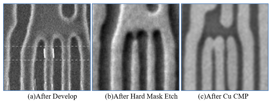
In addition to finding a more accurate process window at every patterning step, a number of failing patterns were also found that showed a clear defect progression across fabrication processes, as shown in Figure 8.


Figure 8.   
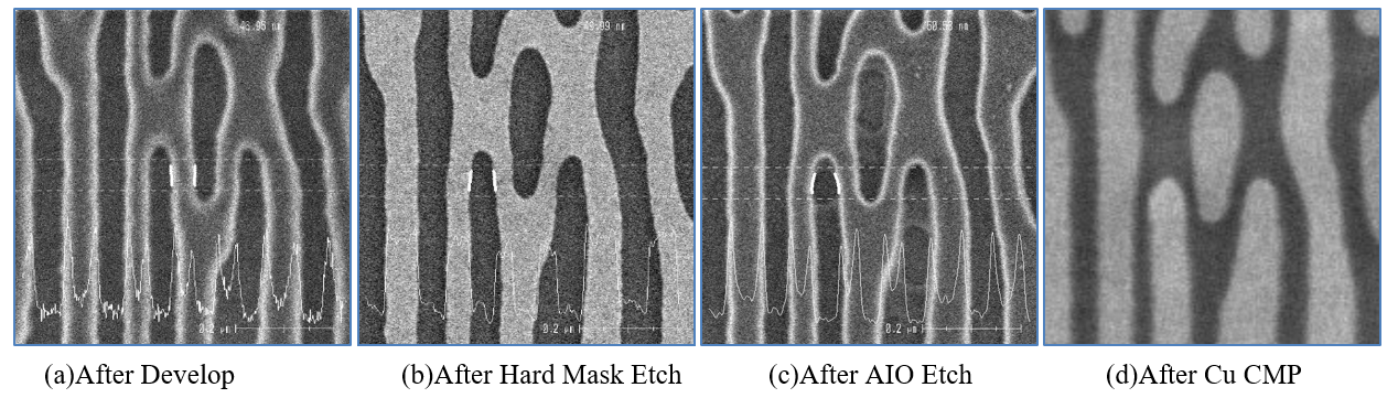
Example of pattern defect detected by D2DB-Pattern Monitor solution.
As a result of the vast amount of feature size and defect information collected and processed, feedback was provided to the design and OPC control teams. They updated the key impacted features and provided an improved version of the reticle. Validation of the revised reticle was also done using the same D2DB-PM methodology and confirmed that the known failing patterns were fixed and that the process window had been improved. An example of a process problem that was originally detected is shown in Figure 5, and its confirmed fix is shown in Figure 9.


Figure 9.   Example of monitoring after process fix
4.   Conclusion
The process integration team encountered a challenging patterning problem that was cumbersome to solve using the conventional methods. The pattern-centric D2DB-PM solution was utilized to first understand the patterning issue thoroughly. The automated image processing functions of D2DB-PM allowed us to collect and analyze a significantly increased number of critical patterns from the full chip design. The turnaround time for determining the process window was drastically reduced from about 80 hours to 4 hours (20x efficiency improvement) with detailed classification of patterns in and around the process window. The capability to measure anywhere within the SEM field of view helped to increase the number of measurement sites without significantly increasing the number of SEM images. The easy visualization and data analysis capabilities provided by D2DB-PM help tremendously to work across process teams to improve and fix specific issues. Because the D2DB-PM flow continuously captures snapshots of various process steps, it is able to flag any subtle change in behavior, and provides a means to monitor the impact of process revisions in the line.
[1] Gyun Yoo, Jungchan Kim, Taehyeong Lee, Areum Jung, Hyunjo Yang, Donggyu Yim, Sungki Park, Kotaro Maruyama, Masahiro Yamamoto, Abhishek Vikram, Sangho Park, "OPC verification and hotspot management for yield enhancement through layout analysis", Metrology, Inspection, and Process Control for Microlithography XXV, Proc. of SPIE Vol. 7971, 79710H (2011).
[2] Taehyeong Lee, Hyunjo Yang, Jungchan Kim, Areum Jung, Gyun Yoo, Donggyu Yim, Sungki Park, Akio Ishikawa, Masahiro Yamamoto, Abhishek Vikram, "Hot spot management through design based metrology: measurement and filtering", Proc. SPIE. Vol. 7520, 75201U (2009).
[3] Eric Guo, Shirley Zhao, Sandy Qian, Guojie Cheng, Abhishek Vikram, Ling Li, Ye Chen, Chingyun Hsiang, Gary Zhang, Bo Su, "Simulation based mask defect repair verification and disposition" Proc. of SPIE Vol. 7488, 74880G, Photomask Technology (2009).
[4] Jing Zhang, Qingxiu Xu, Xin Zhang, Xing Zhao, Jay Ning, Guojie Cheng, Shijie Chen, Gary Zhang, Abhishek Vikram, Bo Su, "Yield impacting systematic defects search and management", Design for Manufacturability through Design-Process Integration VI, Proc. of SPIE Vol. 8327, 832716 (2012).
[5] Abhishek Vikram, Kuan Lin, Janay Camp, Sumanth Kini, Frank Jin, Vinod Venkatesan, “Inspection of high-aspect ratio layers at sub 20nm node”, Metrology, Inspection, and Process Control for Microlithography XXVII, Proc. of SPIE Vol. 8681, 86811Q (2013).
[6] Ming Tian, Yu Zhang, Tiapeng Guan, Jianghua Leng, Baojun Zhao, Lei Yan, Wei Hua, Abhishek Vikram, Guojie Chen, Hui Wang, Gary Zhang, and Wenkui Liao "Critical defect detection, monitoring and fix through process integration engineering by using D2DB pattern monitor solution", Proc. SPIE 10962, Design-Process-Technology Co-optimization for Manufacturability XIII, 109620L (2019).
[7] Qian Xie, Panneerselvam Venkatachalam, Julie Lee, Zhijin Chen, and Khurram Zafar "Design guided data analysis for summarizing systematic pattern defects and process window", Proc. SPIE 9778, Metrology, Inspection, and Process Control for Microlithography XXX, 97782D (2016).
[8] Weihong Gao, Xuefeng Zeng, Peter Lin, Yan Pan, Ho Young Song, Hoang Nguyen, Na Cai, Zhijin Chen, and Khurram Zafar "Net tracing and classification analysis on E-beam die-to-database inspection", Proc. SPIE 9778, Metrology, Inspection, and Process Control for Microlithography XXX, 97783Q (2016).
[9] Khurram Zafar, Chenmin Hu, Ye Chen, Yue Ma, Chingyun Hsiang, Justin Chen, Raymond Xu, Abhishek Vikram, Ping Zhang, "Pattern weakness and strength detection and tracking during a semiconductor device fabrication process", US Patents #9,846,934 (2017), #10,062,160 (2018).
[10] Khurram Zafar, Chenmin Hu, Ye Chen, Yue Ma, Chingyun Hsiang, Justin Chen, Raymond Xu, Abhishek Vikram, Ping Zhang, "Pattern weakness and strength detection and tracking during a semiconductor device fabrication process", Taiwan Patents #I608427(2017), #I634485 (2018).
Article and author information
Yu Zhang
Abhishek Vikram
Ming Tian
Tianpeng Guan
Jianghua Leng
Baojun Zhao
Lei Yan
Wei Hu
Guojie Chen
Hui Wang
Gary Zhang
Wenkui Liao
Publication records
Published: June 28, 2019 (Versions2
References
Journal of Microelectronic Manufacturing