Research Article Archive Versions 2 Vol 2 (4) : 19020405 2019
Download
The Effect of Fin Structure in 5 nm FinFET Technology
: 2019 - 10 - 16
: 2019 - 12 - 25
2337 64 0
Abstract & Keywords
Abstract: In 5 nm technology node, FinFET device performance is sensitive to the dimension of the device structure such as the fin profile. In this work, we simulate the influence of fin height and fin width to an n-type FinFET. We have found that an optimized fin height lies between 50~60 nm. The threshold voltage shift by quantum confinement effect has a steep increase as fin width shrinks to 4 nm. Sharper fin cross section profile gives better subthreshold swing (SS) and stronger drive current because of better gate control.
Keywords: 5 nm; FinFET; fin profile; semiconductor
1.   Introduction
In the last 40 years, CMOS manufacturing design rules have been continuously shrinking from a few microns to the current a few nanometers. Since Intel Corporation made the first FinFET at 22 nm technology node, TSMC and Samsung have developed the 16/14 nm FinFET logic technology in 2015 [1-3]. As the device evolves to 5 nm technology node and beyond, shorter gate length and smaller critical dimensions will induce more physical effects, such as, ballistic transport, quantum confinement, which will affect device performance besides Short Channel Effect (SCE) and Drain-Induced-Barrier-Lowering (DIBL). Although the fin structure is advantageous in transistor performance gain over planar structure, its fabrication process can be very complicated and challenging. Among all fin dimensions, the height and profile are the most important ones. To the FinFET technology nodes that have been put into production, an increase of the fin height will give drive current boost for smaller design rules. However, it may introduce extra parasitic capacitance. In our study on the 5 nm FinFET devices, it shows that an optimized fin height may lie between 50~60 nm for N-type devices. Besides, the fin profile can also influence FinFET device performance. In device simulation, we have considered the threshold voltage (Vth ) shift induced by quantum confinement effects [4-6]. It has been reported that the quantum confinement effect due to narrow fin width and short gate length may introduce a shift in threshold voltage, around 50 mV at a fin width of 5 nm [7]. We will present an optimized FinFET structure with the consideration of all above factors.
2.   FinFET Fabrication and Profile
In this work, we focus on 5 nm technology node FinFET fabrication. Device critical dimension of advanced technology node will shrink to a certain fraction, generally 0.7× compared to last technology node, to keep Moore’s law moving forward. According to public information [8], key dimension for a typical 5 nm FinFET are listed as follows:
Table 1.   Key parameters of 5 nm FinFET device structure.
ParameterCritical dimension (nm)
Fin pitch24 nm
Gate pitch50 nm
Fin width5 nm
Gate length19 nm
Fin height50 nm
Source/drain epi height50 nm
Channel doping2×1015 cm-3
The FinFET process is simulated by Sentaurus TCAD software [9]. The half of an initial FinFET structure is shown in Figure 1(a). A slice cut of the fin profile across the channel direction in shown in Figure 1(b), which indicates that the top of fin width is 5 nm, the bottom of fin with is 5.5 nm and fin height is 50 nm.


  Figure 1. (a) 3D architecture of half of FinFET. (b) Slice of fin profile cross the channel. The top of fin width is set initially to be 5 nm and bottom at 5.5 nm. The fin height is initially set to 50 nm.
3.   Fin Height Influence on Device Performance
FinFET structure has advanced the MOSFETs due to raised channel and multi-gate control which introduce more effective channel width and the stronger gate control. Since the electrical current mainly flow along the fin, therefore, the fin height can directly influence the drive current of the device. Since the taller fin gives wider effective channel width, the effective channel width can be written,
(1)
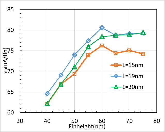
where the H_fin represents fin height and W_fin is width of the fin. Then, more carrier flow along the channel. However, because of the narrow critical dimension of 5 nm FinFET structure, the parasitic capacitance of the device is to a large extent subjected to narrow spacer and extreme thin oxide thickness. Figure 2 shows that the drive current Ion of device increases linearly as the fin height increases from 40 nm to 60 nm, about 22.9%, 24.8%, and 26.1% boost for 15 nm, 19 nm and 30 nm gate length device, respectively. As the fin height reaches over 60 nm, the drive current approaches a saturation value since the source/drain height does not change.


Figure 2.   
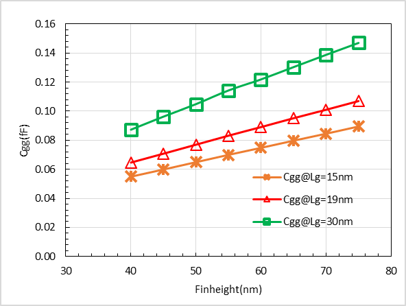
FinFET device drive current boost as the fin height increase.


Figure 3.   Linear increase of the device capacitance Cgg as the fin height increase.
At the same time, the capacitance of device Cgg exhibits a linear rise as the fin height grows from 40 nm to 75 nm. The capacitance is not affected by source/drain height mainly because the capacitance of gate to fin is the main contributor to Cgg . The increase of fin height from 40 nm to 60 nm has introduced 37.7%, 36%, and 39.6% rise in Cgg for 15 nm, 19 nm, and 30 nm gate lengths, respectively. Compared to drive current increase versus fin height, the increase of Cgg is more rapid. However, in manufacturing process, to make a tall fin while keeping the pitch fixed needs challenging high aspect ratio etch and film deposition technologies. As a more advanced technology node over 16/14 nm and 7 nm, the goal for the 5 nm drive current is defined as 70 A/fin. Therefore, we set the optimized fin height between 50 nm to 60 nm, maintaining the drive current goal while the Cgg is not too large.
4. Threshold Voltage Shift by Quantum Confinement Effect
As the fin width shrinks to several nanometers, the dimension confinement causes sub-band splitting due to the Quantum Mechanical (QM) effect. Given a certain gate voltage bias, as it has been reported that the inversion charge density resulted by the sub-band splitting is smaller than the classical (CL) one [6,7], the QM channel potential is lower than the CL one, inducing the Vth shift. The quantum confinement effect caused Vth shift can be described by,
(2)
where the SS represents the subthreshold swing, q is carrier charge, and the represents the difference of channel potential between QM and CL model.


Figure 4.   
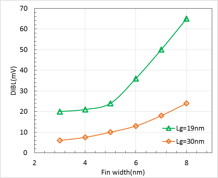
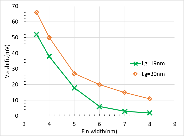
FinFET device DIBL performance as fin width shrinking. Little DIBL due to gate control.


Figure 5.   Simulation results of threshold voltage shift by quantum confinement effect.
The simulation results are shown in Figure 4 and Figure 5. It indicates that, though the device DIBL can benefit from fin width shrink, the Vth shift will become worse by quantum confinement effect. When fin width is large enough, 6 nm for example, the Vth shift is not significant. But, when the fin narrows to 5 nm the Vth shift can be significant, which exhibits a steep Vth increase as the fin continues to shrink, especially when the fin narrows to 4 nm, the \({V}_{th}\) shift can reach 50 mV (19 nm gate length device). Therefore, it is reasonable to keep the fin width at 5 nm or greater.
5.   The Slope of Fin Profile
As concluded from above, in order to continually boost device performance, the fin height can be used to gain drive current, but the fin height may reach a maximum limit as a need to balance the fast increase of capacitance, which may limit the device speed. Beside fin height, we can reduce the leakage current through making more vertical fins because the leakage current happens at bottom of fins. Figure 6 shows that drive current will be enhanced as the fin bottom decreases from 10 nm toward 5 nm with a fixed fin top of 5 nm (triangles with a through line), which will reach about 74 A/fin at a fin bottom width of 5.5 nm. Moreover, SS will drop (diamonds with a through line) down to 73 mV/Dec as well when the slope of fin becomes almost vertical.It can be understood that the shrink of the fin bottom will enhance the gate electric field in channel. For manufacturability consideration, it is not practical to construct a fin with vertical sidewall angle, the current process can support to a maximum of 89 degrees in sidewall angle.


Figure 6.   Fin bottom width shrink results stronger drive current (triangle with a through line) and lower SS (diamonds with a through line) with a fixed fin top of 5 nm.
6.   Conclusion
The fin profiles take an important role in 5 nm technology node and probably beyond due to narrow critical dimensions. Taller fins can provide stronger drive current but will cause more parasitic capacitance. As a result of our study, the optimized fin height lies between 50 nm to 60 nm. The narrow fin gives better DIBL performance, however, it also causes Vth increase by quantum confinement effect. A significant Vth shift will start at 5 nm fin width and will increase steeply when the fin width goes below. It is advantage to make more vertical Fin profile because the steeper slope of fin profile can provide better gate control, larger drive current, and lower SS.
Acknowledgments
We thank the higher management team from Shanghai IC R&D Company for the support of this work.
[1] S. Natarajan, et.al, “A 14nm logic technology featuring 2nd-generation FinFET, air-gapped interconnects, self-aligned double patterning and a 0.0588 µm2 SRAM cell size,” IEEE, IEDM 14, pp. 71-74 (2014).
[2] S. Y. Wu, et. al, “Mayfield Handbook of Technical and Scientific Writing A 16nm FinFET CMOS Technology for Mobile SoC and Computing Applications,” IEEE, IEDM 13, pp.224-227 (2013).
[3] S. Y. Wu et al., “An Enhanced 16nm CMOS Technology Featuring 2nd Generation FinFET Transistors and Advanced Cu/low-k Interconnect for Low Power and High Performance Applications,” IEEE, IEDM 4, pp. 48-51 (2014).
[4] Y. K. Choi, et al., “Threshold Voltage Shift by Quantum Confinement in Ultra-thin Body Device,” device research conference, pp.85-86 (2001) (1953).
[5] J. B. Roldán, et. al, “An Analytical I–V Model for Surrounding-Gate Transistors That Includes Quantum and Velocity Overshoot Effects,” IEEE, TED57, pp. 2925-2933, (2010).
[6] V. P. Trivedi, et.al, “Quantum-Mechanical Effects on the Threshold Voltage of Undoped Double-Gate MOSFETs,” IEEE, IEDM 26, pp. 579-582 (2005).
[7] G. Mei, et. al, “Quantum mechanical effects on the threshold voltage of surrounding-gate MOSFETs,” Microelectronics Journal, 43 , pp. 894–897 (2012)
[8] China Semiconductor Forum.
[9] Sentaurus Process User Guide I-2018.06, Synopsys Inc., Mountain View, CA, USA, (2018).
Article and author information
Enming Shang
Yu Ding
Wenqiao Chen
Shaojian Hu
Shoumian Chen
Publication records
Published: Dec. 25, 2019 (Versions2
References
Journal of Microelectronic Manufacturing