Research Article Current Issue Versions 2 Vol 3 (4) : 20030408 2020
Download
Machine Learning based Optical Proximity Correction Techniques
: 2020 - 10 - 09
: 2020 - 12 - 15
: 2020 - 12 - 30
2250 81 0
Abstract & Keywords
Abstract: The shrinking of the size of the advanced technological nodes brings up new challenges to the semiconductor manufacturing community. The optical proximity correction (OPC) is invented to reduce the errors of the lithographic process. The conventional OPC techniques rely on the empirical models and optimization methods of iterative type. Both the accuracy and computing speed of the existing OPC techniques need to be improved to fulfill the stringent requirement of the research and design for latest technological nodes. The emergence of machine learning technologies inspires novel OPC algorithms. More accurate forward simulation of the lithographic process and single turn optimization methods are enabled by the machine learning based OPC techniques. We discuss the latest progress made by the OPC community in the process simulation and optimization based on machine learning techniques.
Keywords: optical proximity correction; machine learning; deep learning; lithography
1.   Introduction
Optical proximity correction (OPC) becomes critical for the process of current advanced technological nodes. The conventional methods of the optical proximity correction rely on the empirical rules or the combination of the parametric models and traditional optimization methods most likely in the iterative sense. The empirical rules highly depend on the experience of process engineers and works well for the early technological nodes with larger critical dimensions, but the model based methods are required for the sub 100nm technological nodes. Considering the difficulty of the rigorous mathematical simulation of the physical and chemical process involved in the optical lithographic process, simplified models with empirical parameters are usually applied in the actual OPC process[1, 2]. Even the contemporary numerical methods such as Finite Difference Time Domain (FDTD)[35] or Finite Element Method (FEM) et. al. are able to provide more accurate solutions to the optical imaging process, photo-chemical reactions and so on, the formidable cost of computation power hinders the application of such methods to larger scale systems such as full chip level optimization problems. The past efforts in deriving more accurate analytical or semi-numerical models for the forward simulations of relevant physical chemical processes[6,7] boost the development of more practical and efficient OPC technologies. Even the complexity of the photo-resist reactions slows down the progress of obtainment of more reliable resist model, and so does the etch model, the optical imaging problems can usually be well resolved after simplified assumptions are made to the optical imaging systems. The appearance of the computational tractable models makes the iterative optimization of the mask shapes possible which becomes the corner stone of the current OPC technologies. Combining with the latest setup of the optical lithography machines which enables the variable illumination conditions[8, 9], source-mask optimization (SMO)[1012] also becomes an important part of the OPC workflow. Until the techniques of the insertion of sub-resolution assist features (SRAF) being added to the arsenal of OPC toolkit to enlarge the process window of the optimized mask patterns, the framework of contemporary OPC is settled down. However, the room of the improvement of current OPC workflow remains and the rise of data science as well as machine learning provides huge amount of opportunities for the computational lithography community.
2.   Optical Lithographic System


Figure 1.   Illustration of an optical lithographic projection system[13].
The optical microlithography system mainly includes four parts: source, mask/reticle, exposure system and wafer. To avoid the inhomogeneity of illumination on the photomask, Kohler’s method of illumination is applied. The source or the image of the source is placed at the focal plane of the condenser. The photomask/reticle is then illuminated by the parallel beam and the energy distribution on the top plane of the mask is then homogenous in the idealistic situation. Traditional mask is the binary intensity mask. They are formed by the chromium on glass. Different types of fused silicon are applied for varied illumination wavelengths. Phase shift masks are also introduced to improve the image quality. The image of the scattering sources on the photomask is formed on the wafer after the projection optics. The standing wave pattern is formed by the reflection from the photoresist/wafer interface. There are two types of photoresist: positive resist and negative resist. They response differently to the illumination.
3.   Machine Learning Based OPC
The machine learning and data driven perspective may change the OPC workflow mainly in three aspects. Firstly, more accurate and fast models become accessible after the introduction of novel tools such as deep neural networks as a good universal approximator which should be beneficial even they are simply embedded into the traditional OPC framework; Secondly, the expensive and time consuming iterative optimization process of prevailing OPC techniques may be replaced by the single run computation of well trained models which directly perform the optimization process including the mask optimization (MO), SMO, SRAF insertion and so on; Third, the whole workflow of the OPC may be modified by the data driven methodology and the changes may not be constrained within the scopes of feature pattern selection and hotspots detection. The novel full chip level solution may be enabled in the future. We shall discuss the recent progress of the machine learning based OPC technologies in the three directions mentioned above separately.
3.1.   Machine Learning Based Simulators
The simulation of the lithography mainly contains three parts: Optical model, Resist model and Etch model. The first two process is coarsely shown in Figure 1.


Figure 2.   Lithography simulation[14].
The ideal situation of the forward simulation is the success of the ab initio calculation. For the optical imaging system, this target is more achievable. The realistic imaging system is usually simplified and mathematical abstraction can be done within the framework of optics[15]. In Figure 2, a typical optical configuration is shown. The aerial image is computed approximately with methods such as Hopkins method et.al. The chemistry involved in the resist model is complicated to compute from the first principle[16-18]. Sometimes, a simple threshold model is applied for the resist model and the threshold can be either constant or variable[19]. The etch model is more intractable due to the complicated physical- chemical process and multi-factorial control parameters involved such as plasma nature, chamber configuration et.al. Historically, variable etch bias (VEB) model is applied for the optimization purpose[20]. However, the approaches mentioned above may not be able to meet the requirement of the OPC techniques developing for the advanced technological nodes and more accurate and rigorous models are necessary while the nodes shrink. The machine learning based resist model and etch model turn out to be effective and becomes good candidates for future OPC application.
The general purpose of the ML based simulators is to obtain a general function approximator with the local geometric features as input and values of the height or threshold at the pixel level as the output. In principle, it can be done with the multilayer neural networks.


Figure 3.   ANN-based 3D resist model[21].
Seongbo Shim et. al. applied the full connected neural network to fit the resist model with the points sampled from the geometry of layout as the input and the resist height at center of the window as the output. The configuration of their model is shown in Figure 3. Youngchang Kim et. al. use the similar method to realize the prediction of etch bias[20].


Figure 4.   CNN architecture[14].
Since the inventions of new architectures of neural networks emerge, more efficient and suitable approaches are fetched by the OPC community to improve the performance of the forward simulators. Yuki Watanabe et. al. use convolutional neural networks which are widely applied in the computer vision computation to estimate the resist pattern instead[14]. The architecture of their net is shown in Figure 4. Since sometimes, the rigorous simulation or experimental data are hard to obtain especially for new technical nodes, to obtain the trained model with the required accuracy with fewer data, Yibo Lin et. al. take the advantage of the transfer learning and active learning while they are trying to solve the same problem[22]. Later, the generative adversarial net is also introduced by the same group for simulating purpose[23].
3.2.   Machine Learning Based Optimizers
Early days, the mask optimization relies on the empirical rules which usually depend on the geometry of the layout patterns. The contours of the layout patterns are decomposed into the edges and corners and the positions of their end points are varied and optimized according to the rules subtracted from the experimental facts[24]. Even though computationally efficient, the rule based optimization methods are not able to provide the required accuracy and fail to fulfill the requests of the advanced technological nodes. A more robust iterative optimization method based on the optical models, photoresist models et. al. is introduced. The basic idea is to change the positions of the end points of the edges and corners mentioned above and the simulated images on the wafer are obtained accordingly. The full optimization cycle is stopped once the target patterns and the simulated images match each other. Different kinds of error functions are applied to provide a quantitative estimation of the deviations between the target patterns and the simulated images. The Edge Displacement Error (EDE)[25], Edge Placement Error (EPE)[26] or Pixel-wise Error Summation[27] et. al. are usually calculated. The optimization process is usually computationally expensive due to the slow convergence of the iterations. While coarser models which are more computationally tractable are applied at the cost of the accuracy, the effort of the reduction of the iterations inspired the early application of machine learning techniques to the OPC regime and it remains as a main purpose of machine learning based OPC packages till nowadays.
The earlier attempt to obtain a better initial guess for the mask optimization process with the linear regression methods done by the researchers at University of California, Berkeley becomes an excellent start point in this track[28]. Taking advantage of the large dataset of the modified mask patterns after OPC by the commercial EDA packages, the authors estimate the expected fragment movement by the simplest linear statistical model provided an input target layout pattern. It provides a prototype of the basic ideas of the machine learning based OPC technologies within the framework of the supervised learning method. The realization of the workflow still requires the involvement of the advanced commercial EDA packages to generate the labeled data (the correct fragment movement given a specific mask pattern as the original input). As a result, the upper bond of the accuracy of this type of method is constrained by the correctness of the simulators and the efficiencies of the optimizers of the relevant commercial software. And the performance of such method is further compromised by the oversimplification of the mapping from the original input mask pattern to the predicted fragment movements by the application of a linear model. However, the trained linear model serves as a coarse optimizer of the input mask pattern which provides the optimized mask pattern in a single run while it is fed by the input feature vectors representing the original mask patterns. The authors successfully reduce the number of iterations of the traditional OPC workflow by the replacement of the original mask pattern with the statistically learned one as the initial condition of the subsequent optimization flow. 
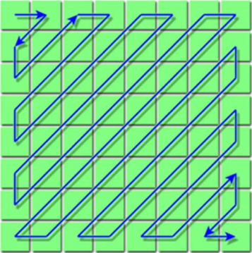
Another significant contribution of the authors is that they successfully introduce a representation method for the input mask layout which makes the further calculation they complete computationally feasible. The discrete cosine transform (DCT) is applied to the input mask layout, and first hundreds of the DCT coefficients is collected in the Zig-Zag order (Shown in Figure 5.) as the input feature vectors of the linear model to be trained.


Figure 5.   Zig–zag ordering of DCT coefficients[28].
The feature engineering accomplished this way serves as one of the mainstream techniques in the OPC community before more efficient and universal feature learning techniques fitting the requirement of the end to end learning such as the prevalent convolutional neural network (CNN) techniques are introduced from the deep learning community. The DCT is also applied by other researchers in the OPC community later in different ways including the variant form of the Fourier Transforms[2932]. Even after the CNN et. al. deep learning techniques are introduced and the representation learning is realized automatically independent of the input data formulations, DCT is sometimes still used as the pre-processed data type as the neural network inputs[33].
The trained models after the supervised learning as the optimizer instead of the traditional iterative optimization circle are further improved mainly in two aspects: more complicated and accurate model instead of the linear statistical model are used to approximate the mapping between the input mask pattern and the optimized mask pattern (the optimization can be in the form of either motions of the specific edge fragment or the modified mask patterns as a whole.); Different feature engineering can be done or the representation learning within the scope of the deep learning can be applied to the mask pattern and the dimensional reduction can be realized in varied ways accordingly[34].
A direct improvement of the representation capability of the linear model has been done by Tetsuaki Matsunawa et. al.[35] by the application of the generalized linear mixed model instead to include the edge type effect. Considering the universal approximation property of the multilayer neural network, replacing the linear model with the typical multilayer neural network becomes another natural choice and has been done by Rui Luo
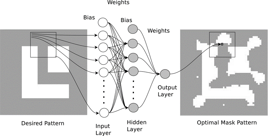
[36]. The author considering the estimation of the binary value of the central pixel of the square modified mask pattern by the standard three layer neural network with the original pixel level binary mask pattern as the input instead of estimating the motion of the central fragment. To obtain the whole modified mask pattern, the author has to scan the three layer model over the original mask pattern. The schematics of the NN is shown in Figure 6. Such kind of scanning can be done naturally by the introduction of the convolutional neural networks and the three layer neural network above can actually be treated as the convolutional layer.


Figure 6.   The schematics of the NN for OPC[36].
The contemporary convolutional neural networks (CNN) with varied architectures have been invented and widely applied to different scenes such as image segmentation, object recognition, image classification et. al.[37]. Basically, it is critical that the actual input of the prevalent CNNs is usually the tensor type data instead of the flatten one used in the Rui’s work, and the convolution layer/Kernel layer with the shared weight parameters slides across the input tensor. The pooling layers are usually applied to further reduce the dimensions of the features learned. After the invention of the training methods of the deep neural networks such as the backpropagation et al.[38], the CNNs emerges. The critical advantage of the deep CNNs is that they permit the representation learned from the multiple levels of the abstraction which are realized by the stacking of varied convolutional kernels and pooling layers. It avoids the necessity of the designing effort of feature engineering by human wisdom and enables the end to end training of models which can be widely applied. The CNNs are immediately fetched by the OPC community and relevant works have been done recently. Once we constrain our discussion within the mask pattern optimization or source optimization problems, the representation of the image patterns by the latent vectors and their decoding are naturally involved and can be directly linked to the encoder-decoder structures. For example, the convolutional autoencoder is trained to do the Source Mask Optimization by Ying Chen et. al.[39] to dramatically raise the speed of the optimization process by a factor of 10
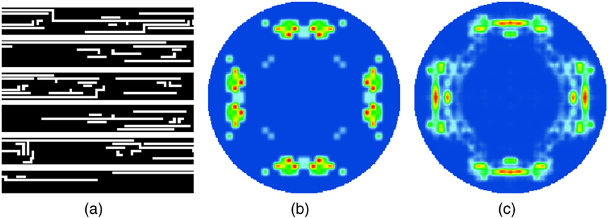
5. Their model output is shown in Figure 7.


Figure 7.   Illustrations of (a) a layout clip, (b) a model-based source, and (c) an autoencoder-based source. [39]
Similarly, the stacking convolutional architectures are also implemented by Haoyu Yang et al.[40] to form the generator and discriminator of the generative adversarial network (GAN)
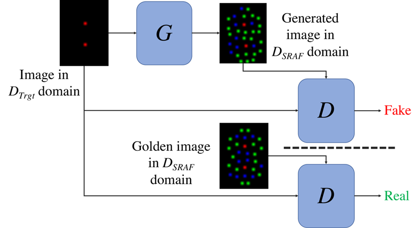
[41] when they succeed in realizing the mask optimization with the modified discriminator design. After the GAN converges, the generator can be used to calculate the optimized mask pattern of the original input one within 0.2s which is negligible compared with the traditional OPC methods. The convolutional autoencoders (CAE) are also applied in other regimes such as the insertion of the Sub Resolution Assist Features (SRAF) et. al.[42]. They can be trained as GAN shown in Figure 8.


Figure 8.   An overview of the CGAN functionality[42].
Basically transformed into a image generation or translation problem
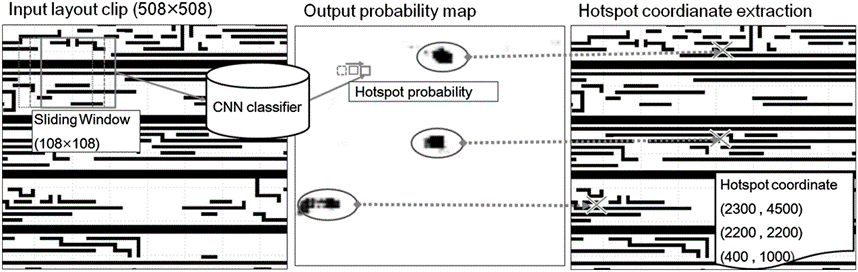
[43, 44], the graphic generation of the modified mask pattern can be done by the mainstream computer vision techniques. Proper modifications made to the design of the specific architectures are necessary. Autoencoders can serve as the models or function approximators of the mapping between the input mask pattern and optimized mask pattern. The training process or the learning of the relevant parameters are finished in the supervise learning mode. In fact, the trained models as the optimizers are not necessarily functioned as the generators of the optimized mask or source patterns. They can also be easily applied as the classifiers for other OPC purposes. We are trying to separate these applications into different categories of OPC techniques although mathematically they are the same in the sense that they eventually act as function approximators providing the appropriate mappings minimizing the designed loss functions. The output can be either mask patterns, source patterns or the labels. We will leave these discussion to the next section where the pattern selection and hotspots detection et. al. are discussed.
3.3.   Machine Learning Modified Workflow
As discussed by Peter De Bisschop[26], the whole OPC workflow strongly depends on the data collection and selection. The main point is: firstly, the feature structures among the billions on the VLSI chip should be selected to build the empirical models unless the physical process is clear enough to be simulated in the first principle way. The latter is rarely the case we confront in the realistic optical lithographic and etching processes. So the establishment and verification of the models as the simulators of the lithographic or etching processes require the data collection and selection even before the machine learning techniques are widely introduced into the OPC regime; secondly, after OPC process, the modified mask patterns or the source conditions should be verified both by the computational method (computational verification) and experimental method (on-wafer verification) before the masks are accepted for the production. As a result, feature pattern selection for the model calibration and on wafer verification et. al. become critical steps. The data sampling problem becomes important for an efficient and robust OPC workflow. The machine learning techniques can solve such kind of problems well. The basic idea is that we should be able to find a proper space defined with correct basis, in which the dimensional reduction of the original data set can be naturally realized. Or, the low dimension manifold in a high dimensional space is discovered and the sampling is done on the manifold only. Both methods can dramatically reduce the required number of sampling points and the cost of the time consuming and expensive computational or experimental verification processes. Dmitry Vengertsev et. al.[45] define a hybrid space formed by the direct sum of image parameter space and geometric sensitivity space and use a modified K means method to cluster the data within the hybrid space. As a typical unsupervised learning method, data clustering helps the selection of the representative patterns and serves as a kind of dimension reduction process. Instead of the K means method, the singular value decomposition (SVD) which can be treated as a form of the principle component analysis (PCA) can also be applied to the matrix representation of the layout patterns defined in the vector space manually constructed[46].
We already discuss the importance of the latent feature vector generation under the background of the machine learning based optimizer. It is also the foundation of the pattern selection we just discussed because the dimension reduction we mentioned is actually finished by the learning of a low dimensional representation of the original dataset. Now, the same thing goes with the hotspots detection. We need to identify the layout structures which can not be manufactured with the acceptable EPE et. al. under the current process conditions and carry out finer OPC for them. We are not able to carry out the forward simulation for all the structures on the chip due to the huge computational power that requires, or we just want a better solution[47]. We are neither satisfied with the traditional pattern match method[48, 49] because it can not predict the hotspot correctly when patterns not included in the library are met. Transforming such problems into the image classification problem[50] and solving it with the prevailing machine learning techniques then become interesting. The basic idea is we learn the low dimensional feature vectoral representation of the layout patterns and use the classifier to distinguish the pattern with hotspots from the pattern without hotspots within certain region in the latent space formed by the learned feature vectors. You can also use them to do data clustering and realize the pattern feature selection. The effectiveness of such kind of method strongly depends on the generalization capability of the machine learning model. It is not well understood when the learned model generalizes well especially when the deep learning techniques are applied. Even without the theoretical guarantee, these machine learning methods are applied in the hotspots detection widely and they are proven effective by the experimental facts. Matsunawa et. al.[51] use the human designed feature vectors to do the classification for the hotspots detection with Adaboost method. Taking advantage of the end to end training capability of deep CNNs, Moojoon Shin[52] et. al. apply different architectures of CNN binary classifier to fulfill the speed and accuracy requirement of hotspots detections. The probability of a pixel being classified as the hotspot is predicted by inputting the image centered at that pixel into the CNN. After scanning the whole layout, the probabilistic distribution of the hotspots at the pixel level is output as the final result. The schematics is shown in Figure 9.


Figure 9.   HS detection using sliding window scan and coordinate extraction[52].
Of course, even CNNs have the advantage in the sense that they automatically include the translational invariance and tend to learn the local information of image while encoding thus dramatically reduce the number of learnable parameters, the general fully connected deep neural network (DNN) can also be applied to carry out the hotspots detection task[53]. To improve the performance of the DNN hotspots detectors, different variants of DNN have been explored[33]. For example, inception mechanism is introduced by Ran Chen et. al.[54]. Haoyu Yang et. al. modifies the CNN architecture and replace all the pooling layers with 3×3 convolution layers[55].
4.   Conclusions
Machine learning techniques especially the deep learning method can dramatically improve the accuracy and computation speed of simulation and optimization process and the full chip level optimization techniques should become available and it will further change the whole workflow of current OPC technology[56].
Acknowledgments
This work is supported by National Science and Technology Major Project of China (2017ZX02315001-003, 2017ZX02101004-003), National Natural Science Foundation of China (61874002, 61804174), Beijing Natural Fund (4182021).
[1] J. W. Thackeray, “Stochastic exposure kinetics of extreme ultraviolet photoresists: simulation study,” J. Micro/Nanolithography, MEMS, MOEMS 10 (3), 033019 (2011).
[2] A. Erdmann, T. Fühner, F. Shao, and P. Evanschitzky, “Lithography simulation: modeling techniques and selected applications,” Model. Asp. Opt. Metrol. II 7390 , 739002 (2009).
[3] A. K. Wong and A. R. Neureuther, “Mask Topography Effects in Projection Printing of Phase-Shifting Masks,” IEEE Trans. Electron Devices 41 (6), 895–902 (1994).
[4] P. Evanschitzky and A. Erdmann, “Three dimensional EUV simulations: a new mask near field and imaging simulation system,” 25th Annu. BACUS Symp. Photomask Technol.5992 , 59925B (2005).
[5] K. Adam and A. R. Neureuther, “Domain decomposition methods for the rapid electromagnetic simulation of photomask scattering,” J. Microlithogr. Microfabr. Microsystems1 (3), 253–269 (2002).
[6] J. Byers, J. Petersen, and J. Sturtevant, “Calibration of Chemically Amplified Resist Models,” Proc. SPIE2724 , 156–162 (1996).
[7] A. Erdmann, G. Citarella, P. Evanschitzky, H. Schermer, V. Philipsen, and P. De Bisschop, “Validity of the Hopkins approximation in simulations of hyper-NA (NA>1) line-space structures for an attenuated PSM mask,” Opt. Microlithogr. XIX 6154, 61540G (2006).
[8] S. M. Kim, S. J. Kim, C. J. Bang, Y. M. Ham, and K. H. Baik, “Optimization of dipole off-axis illumination by 1st-order efficiency method for sub-120 nm node with KrF lithography,” Japanese J. Appl. Physics, Part 1 Regul. Pap. Short Notes Rev. Pap.39 (12 B), 6777–6780 (2000).
[9] S. Suh, Y. Kang, I. Kim, S. Woo, H. Cho, and J. Moon, “Pattern type specific modeling and correction methodology at high NA and off-axis illumination,” 25th Annu. BACUS Symp. Photomask Technol. 5992(2005), 599220 (2005).
[10] H. Aoyama, Y. Mizuno, N. Hirayanagi, N. Kita, R. Matsui, H. Izumi, K. Tajima, J. Siebert, W. Demmerle, and T. Matsuyama, “Impact of realistic source shape and fiexibility on source mask optimization,” J. Micro/Nanolithography, MEMS, MOEMS13 (1), 011005 (2014).
[11] N. Jia and E. Y. Lam, “Pixelated source mask optimization for process robustness in optical lithography,” Opt. Express19 (20), 19384 (2011).
[12] R. Socha, X. Shi, and D. LeHoty, “Simultaneous source mask optimization (SMO),” Photomask Next-Generation Lithogr. Mask Technol. XII 5853, 180 (2005).
[13] A. K. Wong, Resolution Enhancement Techniques in Optical Lithography, SPIE press (2001)
[14] Y. Watanabe, T. Kimura, T. Matsunawa, and S. Nojima, “Accurate Lithography Simulation Model based on Convolutional Neural Networks,” Opt. Microlithogr. XXX 10147, 101470K (2017).
[15] A. K. Wong, Optical Imaging in Projection Microlithography, SPIE press (2005).
[16] C.M. Garza, C.R. Szmanda, and R.L. Fischer Jr., “Resist dissolution kinetics and submicron process control” Proceedings of SPIE: Advances in Resist Technology and Processing V 920 , 321–338. (1988)
[17] K. Itoh, K. Yamanaka, H. Nozue, and K. Kasama, “Dissolution kinetics of high resolution novolac resists” Proceedings of SPIE: Advances in Resist Technology and Processing VIII 1466 , 485–496.(1991)
[18] C.A. Mack, M.J. Maslow, R. Carpio, and A. Sekiguchi, New model for the effect of developer temperature on photoresist dissolution, Proceedings of SPIE: Advances in Resist Technology and Processing XV3333 , 1218–1231. (1998)
[19] Y. Granik, N. B. Cobb, and T. Do, “Universal process modeling with VTRE for OPC,” Opt. Microlithogr. XV 4691(2002), 377 (2002).
[20] Y. Kim, S. Jung, D. Kwak, V. Liubich, and G. Fenger, “Predictable etch model using machine learning,” Opt. Microlithogr. XXXII 10961, 1096106 (2019).
[21] S. Shim, S. Choi, and Y. Shin, “Machine learning-based 3D resist model,” Opt. Microlithogr. XXX 10147(March 2017), 101471D (2017).
[22] Y. Lin, M. Li, Y. Watanabe, T. Kimura, T. Matsunawa, S. Nojima, and D. Z. Pan, “Data Efficient Lithography Modeling with Transfer Learning and Active Data Selection,” IEEE Trans. Comput. Des. Integr. Circuits Syst. 38 (10), 1900–1913 (2019).
[23] W. Ye, M. B. Alawieh, Y. Lin, and D. Z. Pan, “LithoGAN: End-to-end lithography modeling with generative adversarial networks,” Proc. - Des. Autom. Conf. 2019 (2019).
[24] J. Park, C. Park, S. Rhie, Y. Kim, M. Yoo, J. Kong, H. Kim, and S. Yoo, “An Efficient Rule based OPC Approach Using a DRC tool for 0.18 um ASIC,” Proc. IEEE First Int. Symp. Qual. Electron. Des., 81–85 (2000).
[25] W. Ye, M. B. Alawieh, Y. Lin, and D. Z. Pan, “LithoGAN: End-to-End Lithography Modeling with Generative Adversarial Networks,” Proc. DAC107 , 1–6 (2019).
[26] P. De Bisschop, “Optical proximity correction : A cross road of data flows Characteristics in Extreme Ultraviolet Lithography,” Jpn. J. Appl. Phys.55 , 06GA01 (2016).
[27] Y. Shen, N. Jia, N. Wong, and E. Y. Lam, “Robust level-set-based inverse lithography,” Opt. Express 19 (6), 5511 (2011).
[28] A. Gu and A. Zakhor, “Optical proximity correction with linear regression,” IEEE Trans. Semicond. Manuf.21 (2), 263–271 (2008).
[29] S. Shim and Y. Shin, “Topology-oriented pattern extraction and classification for synthesizing lithography test patterns,” J. Micro/Nanolithography, MEMS, MOEMS14 (1), 013503 (2015).
[30] T. Matsunawa, B. Yu, and D. Z. Pan, “Laplacian eigenmaps- and Bayesian clustering-based layout pattern sampling and its applications to hotspot detection and optical proximity correction,” J. Micro/Nanolithography, MEMS, MOEMS15 (4), 043504 (2016).
[31] S. Shim, W. Chung, and Y. Shin, “Synthesis of lithography test patterns through topology-oriented pattern extraction and classification,” Des. Co-optimization Manuf. VIII 9053, 905305 (2014).
[32] W. Zhang, X. Li, S. Saxena, A. Strojwas, and R. Rutenbar, “Automatic clustering of wafer spatial signatures,” Proc. - Des. Autom. Conf., 1–6 (2013).
[33] H. Yang, J. Su, Y. Zou, Y. Ma, B. Yu, and E. F. Y. Young, “Layout Hotspot Detection with Feature Tensor Generation and Deep Biased Learning,” IEEE Trans. Comput. Des. Integr. Circuits Syst.38 (6), 1175–1187 (2019).
[34] G. Hinton and R. Salakhutdinov, “Reducing the Dimensionality of Data with Neural Networks,” Science (80-. ). 313(July), 504–507 (2006).
[35] T. Matsunawa, B. Yu, and D. Z. Pan, “Optical proximity correction with hierarchical Bayes model,” Opt. Microlithogr. XXVIII 9426, 94260X (2015).
[36] R. Luo, “Optical proximity correction using a multilayer perceptron neural network,” J. Opt. (United Kingdom) 15(7) (2013).
[37] W. Rawat and Z. Wang, “Deep Convolutional Neural Networks for Image Classification: A Comprehensive Review,” Neural Comput.29 , 2352–2449 (2017).
[38] Y. Lecun, Y. Bengio, and G. Hinton, “Deep learning,” Nature 521 (7553), 436–444 (2015).
[39] Y. Chen, Y. Lin, L. Dong, T. Gai, R. Chen, Y. Su, Y. Wei, and D. Z. Pan, “SoulNet: ultrafast optical source optimization utilizing generative neural networks for advanced lithography,” J. Micro/Nanolithography, MEMS, MOEMS18 (04), 1 (2019).
[40] H. Yang, S. Li, Z. Deng, Y. Ma, B. Yu, and E. F. Y. Young, “GAN-OPC: Mask Optimization with Lithography-guided Generative Adversarial Nets,” IEEE Trans. Comput. Des. Integr. Circuits Syst. (2019).
[41] I. J. Goodfellow, J. Pouget-Abadie, M. Mirza, B. Xu, D. Warde-Farley, S. Ozair, A. Courville, and Y. Bengio, “Generative adversarial nets,” Adv. Neural Inf. Process. Syst. 3 (January), 2672–2680 (2014).
[42] M. B. Alawieh, Y. Lin, Z. Zhang, M. Li, Q. Huang, and D. Z. Pan, “GAN-SRAF: Sub-Resolution Assist Feature Generation using Generative Adversarial Networks,” IEEE Trans. Comput. Des. Integr. Circuits Syst.(i), 1–6 (2020).
[43] M. Mirza and S. Osindero, “Conditional Generative Adversarial Nets,” 1–7 (2014). http://arxiv.org/abs/1411.1784.
[44] P. Isola, J. Zhu, T. Zhou, and A. A. Efros, “Image-to-Image Translation with Conditional Adversarial Networks,” IEEE Conf. Comput. Vis. Pattern Recognit., 1063–6919 (2017).
[45] D. Vengertsev, K. Kim, S.-H. Yang, S. Shim, S. Moon, A. Shamsuarov, S. Lee, S.-W. Choi, J. Choi, and H.-K. Kang, “The new test pattern selection method for OPC model calibration, based on the process of clustering in a hybrid space,” Photomask Technol.2012 8522, 85221A (2012).
[46] Y. Sun, Y. M. Foong, Y. Wang, J. Cheng, D. Zhang, S. Gao, N. Chen, B. Il Choi, A. J. Bruguier, M. Feng, J. Qiu, S. Hunsche, L. Liu, and W. Shao, “Optimizing OPC data sampling based on ‘orthogonal vector space,’” Opt. Microlithogr. XXIV 7973, 79732K (2011).
[47] J. Kim and M. Fan, “Hotspot detection on post-OPC layout using full-chip simulation-based verification tool: a case study with aerial image simulation,” 23rd Annu. BACUS Symp. Photomask Technol.5256 , 919 (2003).
[48] W. Y. Wen, J. C. Li, S. Y. Lin, J. Y. Chen, and S. C. Chang, “A fuzzy-matching model with grid reduction for lithography hotspot detection,” IEEE Trans. Comput. Des. Integr. Circuits Syst. 33 (11), 1671–1680 (2014).
[49] Y. T. Yu, Y. C. Chan, S. Sinha, I. H. R. Jiang, and C. Chiang, “Accurate process-hotspot detection using critical design rule extraction,” Proc. - Des. Autom. Conf., 1167–1172 (2012).
[50] A. Krizhevsky, I. Sutskever, and G. E. Hinton, “ImageNet classification with deep convolutional neural networks,” Commun. ACM 60(6), 84–90 (2017).
[51] T. Matsunawa, J.-R. Gao, B. Yu, and D. Z. Pan, “A new lithography hotspot detection framework based on AdaBoost classifier and simplified feature extraction,” Des. Co-optimization Manuf. IX 9427, 94270S (2015).
[52] M. Shin and J.-H. Lee, “Accurate lithography hotspot detection using deep convolutional neural networks,” J. Micro/Nanolithography, MEMS, MOEMS15 (4), 043507 (2016).
[53] T. Matsunawa, S. Nojima, and T. Kotani, “Automatic layout feature extraction for lithography hotspot detection based on deep neural network,” Des. Co-optimization Manuf. X 9781, 97810H (2016).
[54] R. Chen, W. Zhong, H. Yang, H. Geng, X. Zeng, and B. Yu, “Faster region-based hotspot detection,” Proc. - Des. Autom. Conf., 0–5 (2019).
[55] H. Yang, Y. Lin, B. Yu, and E. F. Y. Young, “Lithography hotspot detection: From shallow to deep learning,” Int. Syst. Chip Conf. 2017-Septe, 233–238 (2017).
[56] I. Torunoglu, A. Karakas, E. Elsen, C. Andrus, B. Bremen, B. Dimitrov, and J. Ungar, “A GPU-based full-chip inverse lithography solution for random patterns,” Des. Manuf. through Des. Integr. IV 7641(April 2010), 764115 (2010).
Article and author information
Pengpeng Yuan
Pengpeng Yuan received his BS degree in Integrated circuits engineering from Tsinghua University, Beijing, China. He is currently working toward the Ph.D. degree in Institute of Microelectronics of the Chinese Academy of Science, Beijing, China. His research interests include computational imaging, lithographic resolution enhancement based on deep learning.
Taian Fan
Taian Fan is a research assistant at IMECAS (Institution of Microelectronics Chinese Academy of Science). He received his BS in Electrical Engineering from the Beijing Jiaotong University in 2013, and his Ms. degree in Electrical Engineering from the University of Vermont in 2016. His current research interests include Computational Lithography, Computational Electrodynamics and Design/Simulation automation.
Yaobin Feng
Yaobin Feng is senior director in charge of Lithography in YMTC, he joined YMTC in charge of Lithography technology development since 3D NAND project kicked off in 2015. He graduated from Shanghai Jiaotong University as MBA and Southeast University as Bachelor of Automation. Before joining YMTC, He worked in Micron, UMC and ASMC since 2003. He published many papers in computational lithography, lithography process and metrology.
Peng Xu
xupeng2019@ime.ac.cn
Peng Xu received his BS degree in Applied Physics from Harbin Institute of Technology, China and PhD degree in Physics from College of William and Mary, USA. He was a postdoctoral scholar in Institute of Physics, Chinese Academy of Science. He is currently an associate professor at IMECAS. His research interests include computational lithography, near field optical imaging and optical spectroscopy.
Yayi Wei
weiyayi@ime.ac.cn
Yayi Wei is a “Ten Thousand Talents Plan” professor at IMECAS, and he also serves as the director of the Computational Lithography R&D Center and the Open Laboratory of Zhongguancun, focusing on the computational lithography research for the advanced technology node. Prof. Wei received his Ph.D. from the Max Planck Institute for Solid State Research/Stuttgart University under the guidance of the Nobel Prize winner Klaus von Klitzing. Prior to IMECAS, he worked in many prestigious institutions and enterprises including the Department of Energy's Oak Ridge National Laboratory, Infineon New York R&D Center of the U.S.A. and GLOBALFOUNDRIES New York R&D Center of the U.S.A. Prof. Wei has long been engaged in the research and development of semiconductor devices, materials and processes in the semiconductor lithography field. He led or participated in various projects from the 180nm to 10nm technology node.
Publication records
Published: Dec. 30, 2020 (Versions2
References
Journal of Microelectronic Manufacturing