Research Article Current Issue Versions 2 Vol 3 (4) : 20030405 2020
Download
First-principles Simulations of Tunneling FETs Based on van der Waals MoTe2/SnS2 Heterojunctions with Gate-to-drain Overlap Design
: 2020 - 10 - 06
: 2020 - 12 - 14
: 2020 - 12 - 30
2023 43 0
Abstract & Keywords
Abstract: The electronic properties and transport properties of MoTe2/SnS2 heterostructure Tunneling FETs are investigated by the density functional theory coupled with non-equilibrium Green’s function method. Two dimensional (2D) monolayer MoTe2 and SnS2 are combined to a vertical van der Waals heterojunction. A small staggered band gap is formed in the overlap region, while larger gaps remain in the underlap source and drain regions of monolayer MoTe2 and SnS2 respectively. Such a type-II heterojunction is favorable for tunneling FET. Furthermore, we suggest short stack length and large gate-to-drain overlap to enhance the on-state current suppress the leakage current respectively. The numerical results show that at a low drain to source voltage Vds = 0.05V, On/Off current ratio can reach 108 and the On-state currents is over 20 μA/μm for n-type devices. Our results present that van der Waals heterostructure TFETs can be potential candidate as next generation ultra-steep subthreshold and low-power electronic applications.
Keywords: 2D materials heterojunction; tunnel-FET; gate-to-drain overlap; DFT-NEGF
1.   Introduction
The downscaling of field-effect-transistors (FETs) to sub-5nm and more advanced technical node is following the Moore’s law and approaching their physical limitations with traditional silicon FETs. Recently, the discovery of two-dimensional materials in 2005 [1], has opened a brand-new concept to semiconductor engineers who are seeking new materials for replacing the silicon and improving the performance of semiconductor device. Two-dimensional (2D) material-based semiconductor has been acknowledged as a promising option for the next-generation electronics because of their uniform atomic thickness, smooth surface and excellent gate electrostatic controlling ability. With the development of the significant advances in nanotechnology, in the past few years, 2D material field effect transistors (FETs) have drawn a lot of attentions with several 2D materials, such 2D MoS2 [2-4] , 2D InSe [5, 6], black phosphorus (BP) [7-9], 2D Bi2O2Se [10] and so on [11-14].
The potential of these materials has not been thoroughly investigated, and the development of manufacturing atomically thin van der Walls heterostructures gives rise to new opportunities [11, 14]. More and more experimental works have focused on the properties of plane heterojunction and stacked heterojunction [3]. According to the recently researches, high quality 2D SnS2-based FETs have been measured and their ultrahigh on/off current ratio can reach to 10[8] , which is higher than that of BP and other 2D materials FETs [15, 16]. As for 2D MoTe2 material, it has been fabricated all-2D-based FETs which also can reach quite high mobility (over 20 cm2V-1s-1) and on/off current ratio about 105 [17]. However, 2D materials FETs need to satisfy high speed and low energy dissipation applications, which means a lot of challenges exist [18]. As an alternative application, band-to-band tunneling FETs combine with stacked 2D heterojunction can be potential candidates. Importantly, TFETs can make a breakthrough in subthreshold slope (SS) reduced below 60 mV/dec and have a quite low OFF-state current [19]. In ultra-thin vertical heterojunctions, the tunneling distance is reduced to the minimum, which affords the possibility to achieve higher ON-state current. Furthermore, 2D TFETs can effectively control the leakage of direct source-to-drain tunneling and do not have an influence on band-to-band tunneling because of the staggered band alignment when two layers are stacked together [20-22]. Finally, it is expected that a higher on/off current ratio and lower SS will be achieved while the tunneling occurs between two different monolayer 2D materials.
In this work, we investigate a stacked heterojunction tunneling FET based on van der Waals MoTe2/SnS2 heterojunctions (see Figure 1) with gate-to-drain overlap. MoTe2 and SnS2 are two semiconductors with relatively larger band gaps and their stacked structure has the staggered band alignment which is desired to achieve high on-state tunneling current with acceptable leakages [23, 24]. The two materials have high carrier mobility, i.e., hole mobility of MoTe2 is about 200 cm2V-1s-1[25] and the electron mobility of SnS2 can reach about 1398 cm2V-1s-1 [26]. The type-II heterojunction with a small staggered band gap is formed for tunneling transistors [20]. Furthermore, short stack length and large gate-to-drain overlap (see Figure 2) are proposed to enhance the on-state current suppress the leakage current respectively. We employ the density function theory (DFT) method to study the basic electronic properties of monolayer MoTe2 and SnS2. Then, the transport properties of the double gate stacked structure are calculated by Non-Equilibrium Green's Function (NEGF) method. The merits of the proposed TFET, including local density of state (LDOS), on-state current and SS, are compared with monolayer MoTe2 n-TFET. The device performance of the MoTe2-SnS2 TFETs presents the great potential for future semiconductor applications.
2.   Simulations Methods
Most of previous studies utilize Tight-binding Non-Equilibrium Green's Function (TB-NEGF) method to predict the device performance with new materials and operation mechanisms. It is a good compromise between the computational costs and the coverage of quantum transport feature. For example, one typical TB Hamiltonian employs Slater-Koster (SK) parameters by fitting the electronic structure from DFT method [27]. The transport properties are calculated utilizing the fully quantum mechanical NEGF formalism. Note that DFT includes exchange correlation potentials as well as external potentials, to generate the accurate energy band. However, based on SK parameters by fitting the band of DFT, TB only considers the external potential to self-consistently solve the potential field. The calibration and setup of TB parameter library for new materials can be tedious and tricky. In this work, the calibration-free DFT-NEGF method is used to investigate the tunneling FETs based on van der Waals MoTe2/SnS2 heterojunctions, i.e., using the DFT to calculate the Hamiltonian and electrostatic properties of the device; using NEGF to determine non-equilibrium statistics for constructing density matrix; using real Space numerical methods to calculate transport properties and the boundary conditions for open device structures [28]. High precision can be achieved by using DFT-NEGF, but at expense of computational issues in speed and memory limits.
At present, the mainstream DFT-NEGF programs are able to simulate 5000 atomic-scale structures or devices effectively, but larger-scale computational simulations still have difficulties to overcome. If the number of atoms is further increased, there will be insufficient memory. The scale of parallel processes is another limitation. The parallel computing efficiency is poor as the employed CPU cores are increased. This is mainly due to the inefficient use of computing resources. We develop the DFT-NEGF calculation method for this specific application of MoTe2/SnS2 TFET in the following aspects, 1) the matrix distributed calculation mode is introduced; 2) optimize the Poisson equation and Green's function solution algorithm under specific boundary conditions; 3) at the same time, optimize the linear combination of atomic orbitals (LCAO) basis [28-29] set of each element involved in the tunneling transistor to reduce the matrix dimension without reducing the calculation accuracy and improve the calculation ability. The details are beyond the scope of this paper and will be reported elsewhere. The calculations in this work are based on the Nanodcal packages with the aforementioned updates [28].
3.   Results and Discussions
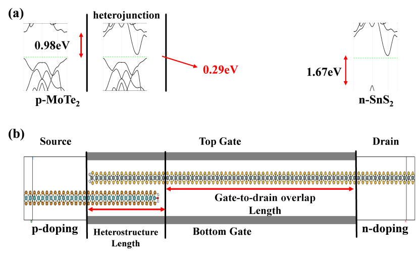
In order to precisely calculate the electronic states properties of the MoTe2-SnS2 heterojunction model, we employ the DFT based ab-initio package Nanodcal. The generalized gradient approximation (GGA) of Perdew, Burke, and Ernzerhof (PBE) is applied for the exchange-correlation interactions, which can exactly present band gap values in good agreement with experiment results for monolayer 2D materials. The energy cutoff is 500 eV and the Monkhorst-Pack k points are set as 9 x 9 x 1 without spin-orbit coupling. The convergence criteria for energy and force are 10-4 eV and 10-3 eV/ Å. The relaxed monolayer MoTe2 and SnS2 are shown in Figure 1 (a) and (b) with the lattice constants being 3.56 Å and 3.70 Å respectively. And the heterostructure is built after applying strain to both two materials so as to obtain the same lattice parameter a0 = 3.625 Å as shown in Figure 1 (c). To study the basic properties of monolayer MoTe2 and SnS2, the band structure of two materials is calculated along the high-symmetry path (K-\(\mathrm{\Gamma }\)-M-K) in Brillouin zones. As shown in Figure 1 (d)-(f), the band structure of intrinsic monolayer MoTe2 has a 1.10 eV direct band gap at K point, like the other traditional 2D semiconductor materials. And monolayer SnS2 has an indirect gap of about 1.61 eV that is an applicable value as the channel material of MOSFETs. Combined two materials, it formed a system that is a type-II heterojunction with a 0.29 eV indirect band gap which is larger than the band gap of another similar combination of 2D material stack, i.e., WTe2-MoS2 (0.16 eV) [23]. Compared all three band structures, it is obvious that the valence band maximum (VBM) is contributed by MoTe2 at K and the conduction band minimum (CBM) is contributed by SnS2 at M. Therefore, if the transport axis is along the M-K direction, the momentum is conserved in the periodic direction and the tunneling process can be formed along the transport direction due to the variation of electrostatic potential.


Figure 1.   (a-c) basic structure of MoTe2, SnS2 and heterostructure, the permittivity cell is covered by the shadow area contained three atoms; (d-f) Band structure and density of states of intrinsic MoTe2, SnS2 and MoTe2-SnS2 heterostructure.
The device band edges schematics demonstrate the mechanism of the MoTe2-SnS2 TFETs as shown in Figure 2 (a). The Type II band alignment can effectively keep the tunneling window of channel. Note that the interaction of the stacking edge has a dramatically deviation of the band structure, as compared with monolayer or heterostructure, which dominate the tunneling on current of the TFET. Longer heterostructure length can hardly enhance the tunneling on current since the bands are rather flat in the middle region, but leads to larger channel resistance. On the other hand, very short heterostructure length also leads to TFEF performance degradation due to the direct source to drain tunneling.


Figure 2.   (a) Band alignment schematic in the device along the transport direction with flat band condition; (b) Schematic of the double-gate MoTe2-SnS2 heterostructure TFETs with gate to drain overlap.
To obtain multi-objective optimization for on-state current and off-state current trade-offs, the schematics of TFETs device with gate-to-drain overlap design is presented in Figure 2(b). The distance between MoTe2 and SnS2 layers is 6.4Å,which is optimized by optB86 exchange correlation functional method. To avoid the influence of mismatch, monolayer MoTe2 is applied 2.1% tensile strain and 2.0% compressive strain is for SnS2, which can keep lowest mismatch. For the whole TFET device structure, the total number of atoms exceeds 360. As shown in Figure 2 (b), the out-of-plane vacuum separation of the device is fixed as 2 nm, which is equal to the distance between the top and bottom gates. Spin-orbit coupling is excluded. In our work, we investigate the influence of EOT variation for the performance of TFETs device. The default effective oxide thickness (EOT) is set to 0.5 nm with effective κ=3.9. For the gate voltage, the bias is only applied to the top gate and the bottom is set as ground. In the case of n-type device, the source side is doped to p-type and the drain side is doped to n-type. Both the source and drain doping concentration reach 1013 cm-2. And the intrinsic materials are employed for the channel because the device performance is insensitive to the doping concentrations. The supply voltage is set as Vds = 0.05 V in all the following simulation. In this condition, the self-consistent electrostatic and transport calculation for each gate bias point spends about 18 hours of wall time by using 144 CPU cores.
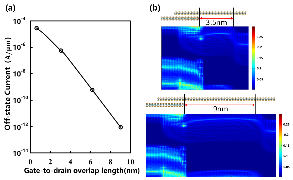
Firstly, we investigate the impact of length variation from heterostructure to drain (gate-to-drain overlap) on the device properties. The heterojunction length is fixed to 3 nm. As shown in Figure 3, the leakage can be effectively reduced with increasing the length of overlap. At Vgs = 0 V, the Off-state current of 4 nm overlap is as large as 10-7A/μm and it can be reduced to 10-13A/μm with 9 nm overlap condition. It indicates that electrons in the VB of MoTe2 have a high probability of tunneling into the CB of SnS2 without gate voltage at short overlap region. The gate-to-drain overlap design gives rise to good optimization for Ion and Ioff trade-offs as compared to normal TFET in previous studies [20] (see Table. 1). The 9 nm gate-to-drain overlap structure is selected as the basic TFET structure to calculate following transport characteristic. In addition, as increasing EOT from 0.5 nm to 1 nm, the performance of TFET device present the degradation tendency, e.g., the subthreshold slope drops to 48 mV/dec and the Ion/Ioff ratio decreases about an order of magnitude. To achieve optimal performance, thin EOT of 0.5 nm is selected in the following calculations.


Figure 3.   
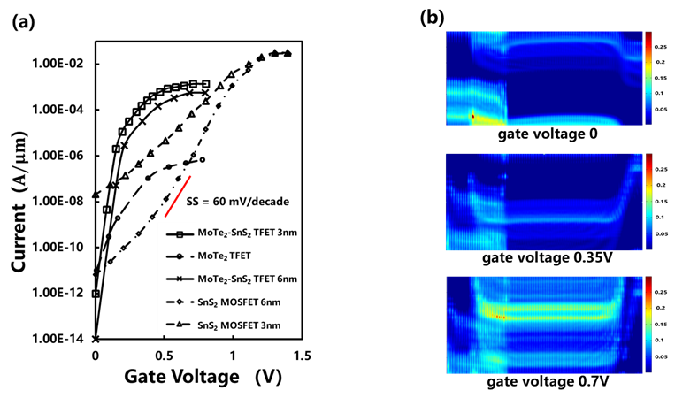
(a) The variation of off-state current with different length of gate-to-drain overlap between heterostructure to drain. With the increasing of length, the leakage of drain can be effectively suppressed at the same supply voltage; (b) LDOS of the TFETs with different gate-to-drain overlap length at Vgs = 0V.
Then, the transport properties of n-type device are simulated by the DFT-NEGF method. The Id-Vgs curve of the MoTe2-SnS2 TFETs is shown in Figure 4 (a). It is obviously that the sub 60 mV/decade subthreshold swing is obtained as about 37 mV/decade. By fixing the Off-state current of the device to\({10}^{-6}\mathrm{ }\mathrm{\mu }\mathrm{A}/\mathrm{\mu }\mathrm{m}\), the current can achieve about 20\( \mathrm{\mu }\mathrm{A}/\mathrm{\mu }\mathrm{m}\). For benchmark, the transfer characteristics of a single-layer MoTe2 TFET is also simulated. The SS is not notably below the limitation of MOSFET and the On/Off current ratio only reach to about 105 due to the short channel length. The mechanism of n-type TFETs is demonstrated in Figure 4 (b), which presents the LDOS of the TFETs with the different gate voltage. At Vgs = 0V, tunneling path does not exist because the VBM of MoTe2 is located below the CBM of SnS2 in the channel region, which also proves that the buffer layers of both two side is long enough to keep the minimal impact of the leakage. With the increasing of gate voltages, the CBM of SnS2 is dropped down faster than the VBM of MoTe2, on account of the effectively modulation of SnS2. At Vgs = 0.35V, electrons in the VB of MoTe2 are gradually enter into the CB of SnS2 at the center of the channel. They can tunnel from the source of MoTe2 cell into the drain because the CBM is getting lower in the monolayer than in the heterostructure. In the On-States, the bands of MoTe2 and SnS2 are totally changed in the overlap region when the gate voltage is over 0.4 V. Electrons can freely cross through the whole stacking area at high gate voltage. This indicates that the MoTe2-SnS2 TFETs can have better performance compared with single-layer 2D materials MOSFETs.


Figure 4.   
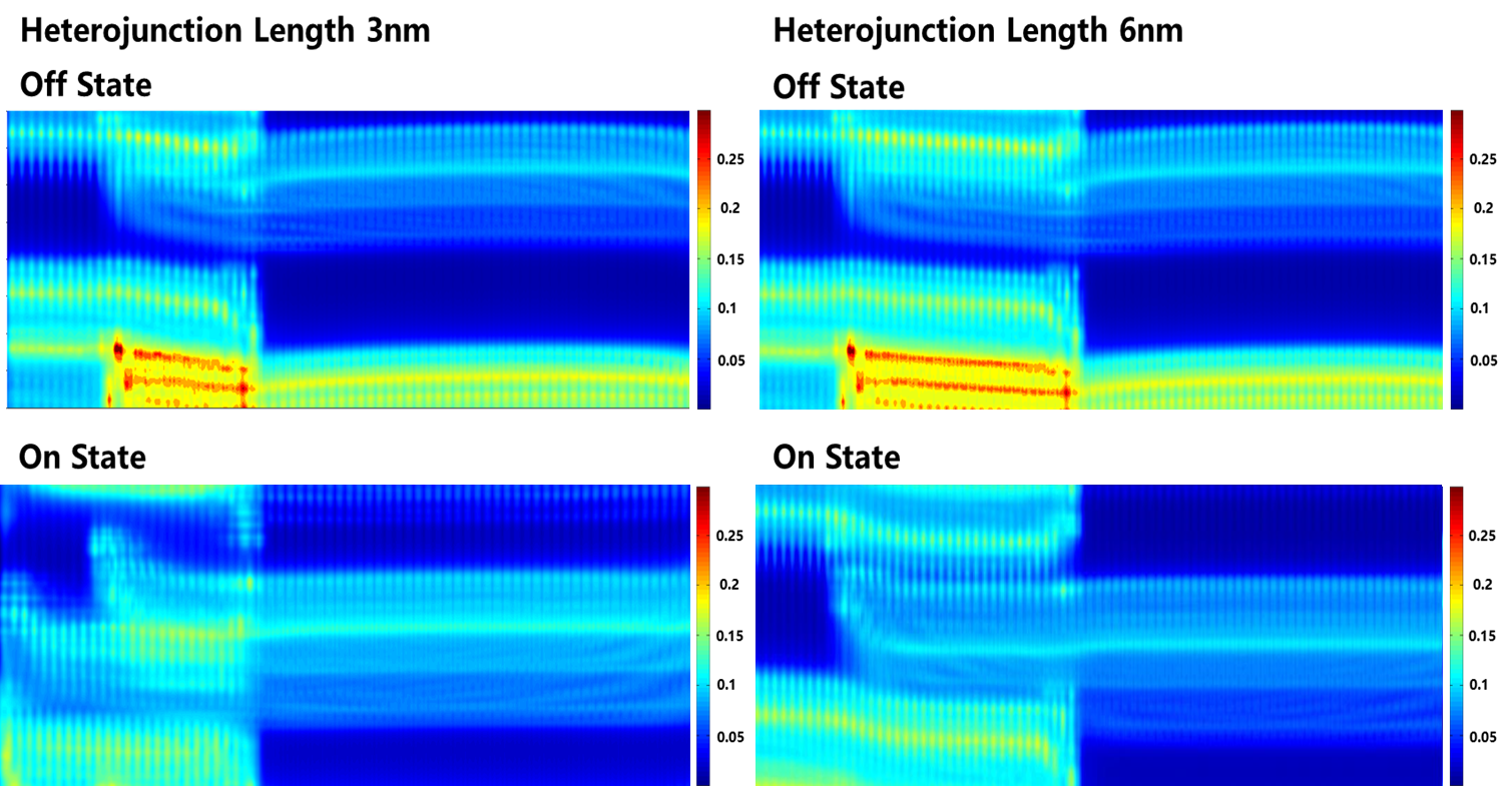
(a) Id -Vgs transfer properties. The solid lines represent the transport characteristics of heterojunction with different heterojunction length region and the dashed lines demonstrate transport properties of single-layer MoTe2 TFET; (b) LDOS of the TFETs with different gate voltages.
Based on this result, we further investigate the influence of increasing the heterojunction region length from 3 nm to 6 nm. On one hand, the length of the stacking region cannot markedly enhance the on-state current. On the other hand, it leads to a better control of the off-state current as shown in Figure 5. As the data presented in Table 1, the on-state current of short heterostructure length TFET is similar to the longer heterojunction length. The band-to-band tunneling and the direct source-to-drain tunneling are essential in the tunneling processes. The longer heterojunction length device can be effectively suppressed the leakage arising from the direct source-to-drain tunneling, but does not notably affect the on-state current due to the band-to-band tunneling.


Figure 5.   LDOS of TFETs with different heterojunction length at On/Off states. At Vgs = 0V, the device of 6nm presents more effective.
Table 1.   Heterojunction length and corresponding device key merits.
Heterojunction Length (nm)Ioff (A/μm)Ion (A/μm)Ion/IoffSS (mV/dec)
3
(this work)
2.05E-125.77E-0410837
6
(this work)
2.38E-141.46E-04101042
20
[Ref 20]
1E-127.5E-5107<60
4.   Conclusion
In this work, we investigate the electronic properties of a MoTe2-SnS2 heterostructure by DFT, which gives rise to a small staggered gap in the stack overlap region and large gap in the source drain. Based on this heterostructure, a double-gate n-type TFET with gate-to-drain overlap has been designed and calculated by DFT-NEGF. At a low supply voltage Vds = 0.05V, On/Off current ratio reaches to 108 and the subthreshold swing is well below the thermal limitation of traditional Silicon MOSFET. It is reasonable that 2D van der Waals heterostructures have a great potential in next generation of ultra-steep subthreshold and low-power applications.
Acknowledgments
This research financially supported by the Training Program of the Major Research Plan of the National Natural Science Foundation of China (61774168, 91964103) and the MOST (2016YFA0202300).
[1] K. Novoselov, D. Jiang, F. Schedin, et al. “Two-dimensional atomic crystals,”PNAS, 102, 10451-10453 (2005).
[2] B. Radisavljevic, A. Radenovic, J. Brivio, et al. “Single-Layer MoS2 Transistors,” Nat. Nanotechnol, 6, 147−150 (2011).
[3] X. Hong, J. Kim, Y. Zhang et al. “Ultrafast charge transfer in atomically thin MoS2/WS2 heterostructures,” Nature nanotechnology, 9, 682-686 (2014).
[4] Y. Pan, Z. Wu, H. Yin, et al. “Near-ideal subthreshold swing MoS2 back-gate transistors with an optimized ultrathin HfO2 dielectric layer”. Nanotechnology, 30, 9, 095202 (2019).
[5] P. Ho, Y. Chang, Y. Chu, et al. “High-Mobility InSe Transistors: The Role of Surface Oxides,” ACS Nano., 11:7362-7370, (2017).
[6] K. Luo, W. Yang, Y. Pan. et al. “Ab-Initio Simulations of Monolayer InSe and MoS2 Strain Effect: From Electron Mobility to Photoelectric Effect,” Journal of Elec Materi, 49, 559–565 (2020).
[7] R. Zhang, Z. Wu, X. Li, et al. “Fano resonances in bilayer phosphorene nanoring”. Nanotechnology, 29, 21, 215202 (2018).
[8] X. Li, K. Luo, Z. Wu, et al. “Tuning the electrical and optical anisotropy of a monolayer black phosphorus magnetic superlattice”. Nanotechnology, 29, 17 174001 (2018).
[9] N. Haratipour, S. Namgung, S. Oh, et al. “Fundamental Limits on the Subthreshold Slope in Schottky Source/Drain Black Phosphorus Field-Effect Transistors,” ACS Nano, 10, 3, 3791–3800 (2016).
[10] P. Luo, F. Wang, K. Liu, et al. “PbSe Quantum Dots Sensitized High-Mobility Bi2O2Se Nanosheets for High-Performance and Broadband Photodetection Beyond 2 mum.” ACS Nano, 13, 9028-9037 (2019).
[11] A. K. Geim and I. V. Grigorieva, “Van der Waals heterostructures,” Nature, 499, 419–425 (2013).
[12] Z. Wu. “Electronic fiber in graphene”. Appl. Phys. Lett., 98,082117 (2011).
[13] Z. Wu, F. Zhai, K. Chang, et al. “Valley-Dependent Brewster Angles and Goos-Ha¨nchen Effect in Strained Graphene”. Phys. Rev. Lett., 106, 176802 (2011).
[14] T. Brumme, M. Calandra, F. Mauri, “First-principles theory of field-effect doping in transition-metal dichalcogenides: structural properties, electronic structure, Hall coefficient, and electrical conductivity,” Phys. Rev. B, 91, 155436 (2015).
[15] S. Wei, C. Ge, L. Zhou, et al., “Performance Improvement of Multilayered SnS2 Field Effect Transistors through Synergistic Effect of Vacancy Repairing and Electron Doping Introduced by EDTA,” ACS Appl. Electron. Mater. 1, 11, 2380–2388 (2019).
[16] D. Chu, S. Pak, E. Kim, “Locally Gated SnS2/hBN Thin Film Transistors with a Broadband Photoresponse,” Sci Rep, 8, 10585 (2018).
[17] K. Choi, Y. Lee, J. Kim, et al. “Non‐Lithographic Fabrication of All‐2D α‐MoTe2 Dual Gate Transistors,” Adv. Funct. Mater. 26: 3146-3153 (2016).
[18] C. Klinkert, Á. Szabó, M. Luisier*, et al. “2-D Materials for Ultrascaled Field-Effect Transistors: One Hundred Candidates under the Ab Initio Microscope,” ACS Nano, 14, 7, 8605–8615 (2020).
[19] Q. Zhang, G. Iannaccone and G. Fiori, "Two-Dimensional Tunnel Transistors Based on Bi2Se3 Thin Film," in IEEE Electron Device Letters. 35, 1, 129-131 (2014).
[20] Á. Szabó, S. J. Koester and M. Luisier, "Ab-Initio Simulation of van der Waals MoTe2–SnS2 Heterotunneling FETs for Low-Power Electronics," in IEEE Electron Device Letters. 36, 5, 514-516 (2015).
[21] K. Lam, X. Cao, and J. Guo, “Device performance of heterojunction tunneling field-effect transistors based on transition metal dichalcogenide monolayer,” IEEE Electron Device Lett. 34, 10, 1331–1333 (2013).
[22] L. Xu, P. Zhang, Z. Hu, et al. “Large‐Scale Growth and Field‐Effect Transistors Electrical Engineering of Atomic‐Layer SnS2,” Small, 15, 1904116 (2019).
[23] J. Cao, M. Pala, D. Esseni, et al, “Operation and Design of van der Waals Tunnel Transistors: A 3-D Quantum Transport Study”, IEEE Transactions on Electron Devices, 63, 11, 4388-4394 (2016).
[24] Á. Szabó, C. Klinkert, D. Campi, et al, "Ab Initio Simulation of Band-to-Band Tunneling FETs With Single- and Few-Layer 2-D Materials as Channels," IEEE Transactions on Electron Devices, 65, 10, 4180-4187 (2018).
[25] S. Mir, V. Yadav, and J. Singh. “Recent Advances in the Carrier Mobility of Two-Dimensional Materials: A Theoretical Perspective”, ACS Omega, 5, 24, 14203-14211 (2020).
[26] A. Shafique, A. Samad and Y. Shin. “Ultra low lattice thermal conductivity and high carrier mobility of monolayer SnS2 and SnSe2: a first principles study”, Phys. Chem. Chem. Phys., 19, 20677-20683 (2017).
[27] A. D. Becke, “Density-functional exchange-energy approximation with correct asymptotic behavior,” Phys. Rev. A, 38, 3098 (1988).
[28] J. Taylor, H. Guo, and J. Wang, “Ab initio modeling of open systems: Charge transfer, electron conduction, and molecular switching of a C60 device,” Phys. Rev. B, 63, 121104 (2001).
[29] J.E. Huheey, E. Keiter, R. Keiter,et al. “Inorganic Chemistry: Principles of Structure and Reactivity”, 4th ed., Dorling Kindersley Pvt Ltd (2008).
Article and author information
Kun Luo
Kun Luo received the M.S. degree of physics from University of Durham, Durham, United Kingdom and the B.S. degree in physics from Shandong University, Jinan, China, in 2015,. In 2017, he became a research intern in Institute of Microelectronics of the Chinese Academy of Sciences. His current research interest includes first principle and TCAD model.
Kui Gong
Kui Gong received the Ph.D. degree in Material Science from the University of Science & Technology Beijing,Beijing, China, in 2015. Meanwhile, as a Joint Ph.D. student research in Condensed Matter Physics department of McGill University, Montreal, Canada, during the period of 2012-2015. He jointed Tech Department, Hongzhiwei Technology (Shanghai) CO., LTD, China, in 2016. Now, he is the manager of Application Technology Department of Hongzhiwei Tech. His current research interests include Quantum transport simulation, TCAD, Density functional theory.
Jiangchai Chen
Jiangchai Chen received the Ph.D degree in Theory Physics from Institute of Physics, Chinese Academy of Sciences, Beijing, China, in 2012. Then he did one-year post-doctor research in the Department of Physics, the University of Hong Kong. In 2015, he joined Technology Department (now the R&D Center), Hongzhiwei Technology (Shanghai) Co., Ltd, Shanghai, China. He is currently responsible for the development of a quantum transport software, Nanoskim.
Shengli Zhang
zhangslvip@njust.edu.cn
Shengli Zhang received his PhD degree from Beijing University of Chemical Technology in 2013. He then joined the Key Laboratory of Advanced Display Materials and Devices, Nanjing University of Science and Technology, where he is a Professor in the Department of Materials Science and Engineering. His research interests focus on electronic devices and applications based on 2D materials.
Yongliang Li
Yongliang Li received the Ph.D. degree from the Institute of Microelectronics, Chinese Academy of Sciences, Beijing, China, in 2011. He was a Staff Engineer with the United Microelectronics Corporation, Singapore, for process integration, from 2011 to 2017. In 2018, he joined the Institute of Microelectronics, Chinese Academy of Sciences, where he is currently a Professor of engineering with the Integrated Circuit Advanced Process Center. His current research interests include high-mobility SiGe/Ge material process integration, and novel 3-D CMOS devices.
Huaxiang Yin
Huaxiang Yin received the B.S. degree in semiconductor physics and devices from Tianjin University, Tianjin, China, in 1996, and the M.S. and Ph.D. degrees in microelectronics and solid-state electronics from the Chinese Academy of Sciences (CAS), Beijing, China, in 1999 and 2003, respectively. From 2003 to 2010, he was with the Samsung Advanced Institute of Technology, South Korea, as a Research Staff Member. In 2010, he joined the Institute of Microelectronics, CAS, where he is currently a Professor with the Integrated Circuit Advanced Process Center and the Key Laboratory of Microelectronics Devices and Integrated Technology. His research interests include nanoscale CMOS devices, VLSI manufacture technology, 2-D materials and devices, and Si X-ray detector.
Zhenhua Wu
wuzhenhua@ime.ac.cn
Zhenhua Wu received the Ph.D. degree in Condensed Matter Physics from the Institute of Semiconductors, Chinese Academy of Sciences, Beijing, China, in 2011. He joined Semiconductor R&D Center, Samsung Electronics, Suwon, Korea, in 2011. In 2016, he became a professor in Chinese Academy of Science in Beijing, China. His current research interests include device physics, TCAD simulation of nanoscale transistors.
Publication records
Published: Dec. 30, 2020 (Versions2
References
Journal of Microelectronic Manufacturing