Authors: Litho World
Keywords:EDA;China
doi:10.33079/jomm.19020305
Abstract:
China's IC industry has been flourishing in recent years, huge market demand together with government investments are the major driving forces for this development. The status and development momen...
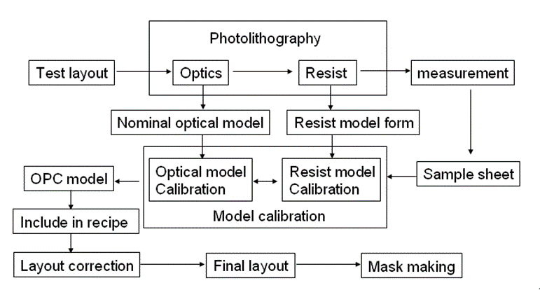
Authors: Qingchen Cao, Tianhui Li, Shuying Wang et al.
Institution:SiEn (QingDao) Integrated Circuits Co., Ltd
Keywords:Image quality;lithography;OPC model;multi-model
doi:10.33079/jomm.19020304
Abstract:
As the process comes into 28nm node and below, lithography struggles stronger between high resolution (high NA) and enough process window especially for hole layers (Contacts and Vias). Taking more...
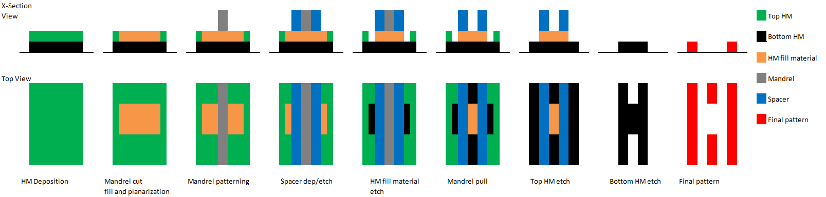
Authors: Jeff Shu
Institution:GLOBALFOUNDRIES
Keywords:self-aligned multiple patterning;SAMP;self-aligned double patterning;SADP;self-aligned quadruple patterning;SAQP;line cut;edge placement error
doi:10.33079/jomm.19020301
Abstract:
Self-aligned multiple patterning (SAMP) can enable the semiconductor scaling before EUV lithography becomes mature for industry use. Theoretically any small size of pitch can be achieved by repeati...
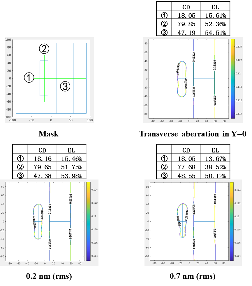
Authors: Yanli Li, Qiang Wu, Shoumian Chen
Institution:Shanghai IC R, &, D Center, 497, Gaosi Road, Zhangjiang Hi, -, Tech Park, China
Keywords:5nm design rule;minimum area;minimum exposure latitude;aberration;shadowing effect
doi:10.33079/jomm.19020406
Abstract:
5 nm logic technology node is believed to be the first node that will adopt Extremely Ultra-Violet (EUV) lithography on a large scale. We have done a simulation study for typical 5 nm logic design ...
Authors: Man Zhang, Liangping Xia, Suihu Dang et al.
Institution:Yangtze Normal University
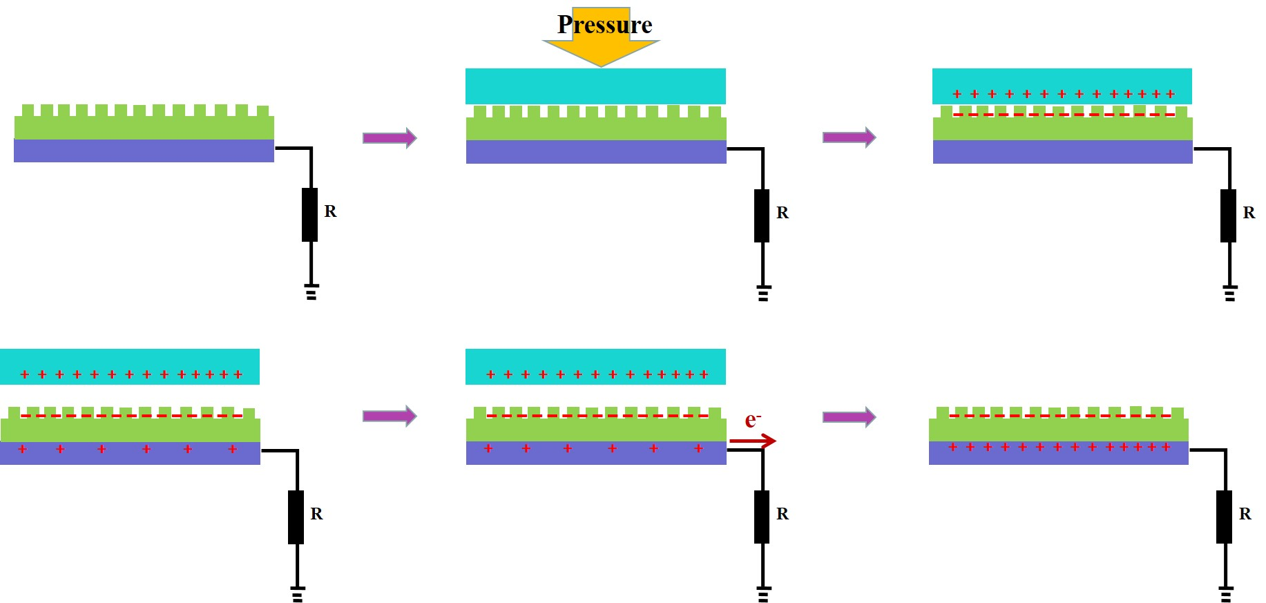
Keywords:Flexible;pressure sensor;poly(dimethylsiloxane);soft nanoimprint lithography;triboelectrostatic charges
doi:10.33079/jomm.19020302
Issue 3: 19020302, 2019
|
PDF
Published: Sept. 26, 2019
Views:4890
Abstract:
This paper proposed a flexible pressure sensor based on poly(dimethylsiloxane) nanostructures film and report an efficient, simple, and low-cost fabrication strategy via soft nanoimprint lithograph...
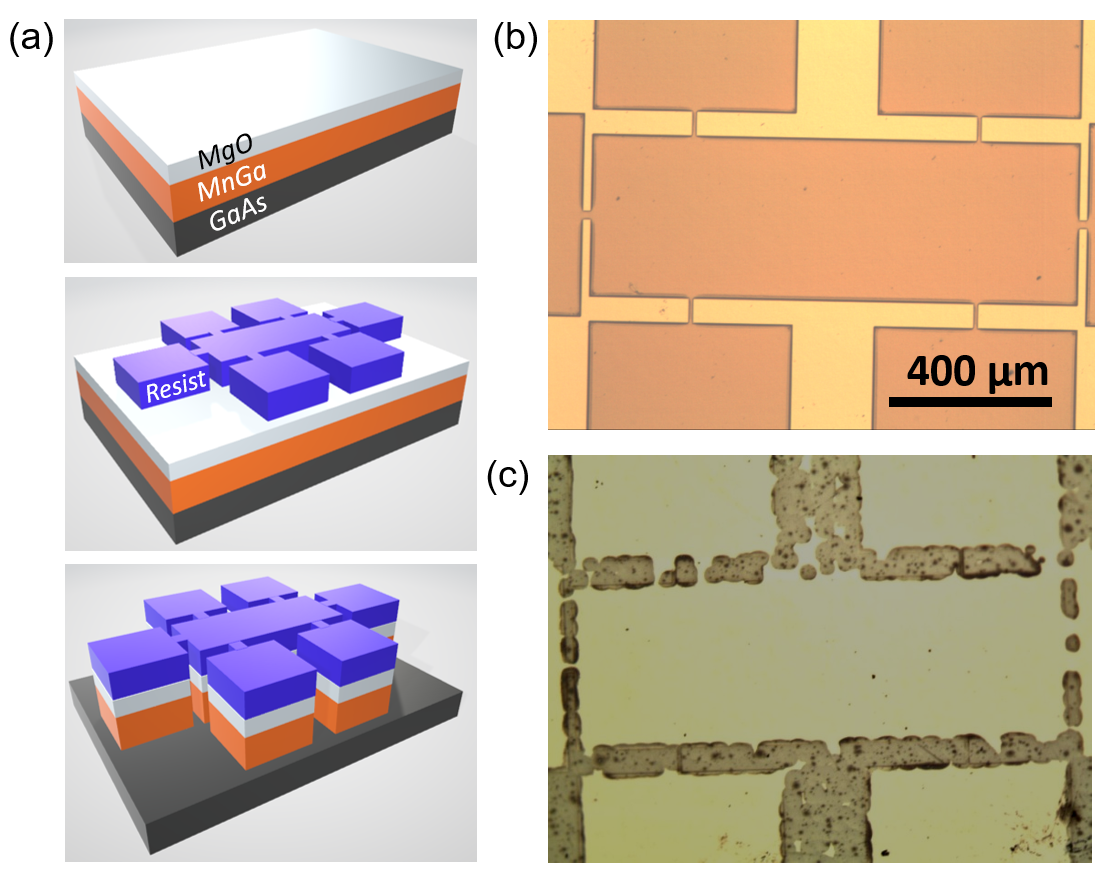
Authors: Lijun Zhu, Jianhua Zhao
Institution:Cornell University
Keywords:Keyword: Chemical stability, Perpendicular magnetic anisotropy, Spintronics, Wet etching
doi:10.33079/jomm.19020303
Issue 3: 19020303, 2019
|
PDF
Published: Sept. 26, 2019
Views:4249
Abstract:
Ferromagnetic films of L10-ordered MnGa have shown promise not only in the applications in ultrahigh-density magnetic recording and spintronic memories, oscillators, and sensors, ...