Authors: Mohamed Baker Alawieh, Yibo Lin, Wei Ye et al.
Institution:Electrical and Computer Engineering, University of Texas at Austin, Austin
Keywords:Design for Manufacturability;Generative Learning;Machine Learning;Lithography
doi:10.33079/jomm.19020401
Abstract:
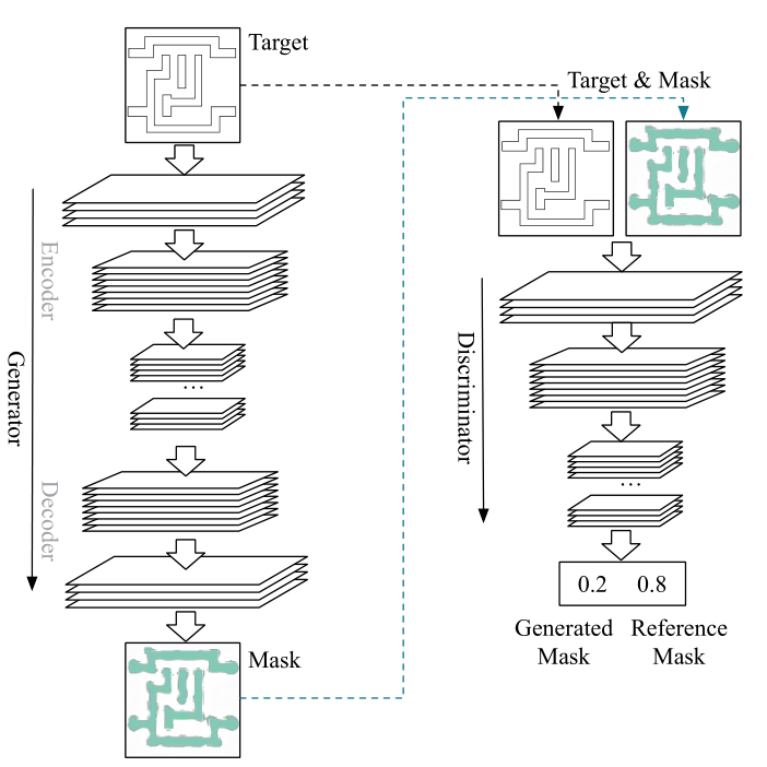
With the continuous scaling of integrated circuit technologies, design for manufacturability (DFM) is becoming more critical, yet more challenging. Alongside, recent advances in machine learning ha...
Authors: Qiang Wu, Yanli Li, Yushu Yang et al.
Institution:Shanghai IC R, &, D Center, 497, Gaosi Road, Zhangjiang Hi, -, Tech Park, China
Keywords:5 nm Logic Process;EUV;SADP;self-aligned LELE;RCWA;stochastics;mask 3D scattering
doi:10.33079/jomm.19020408
Abstract:
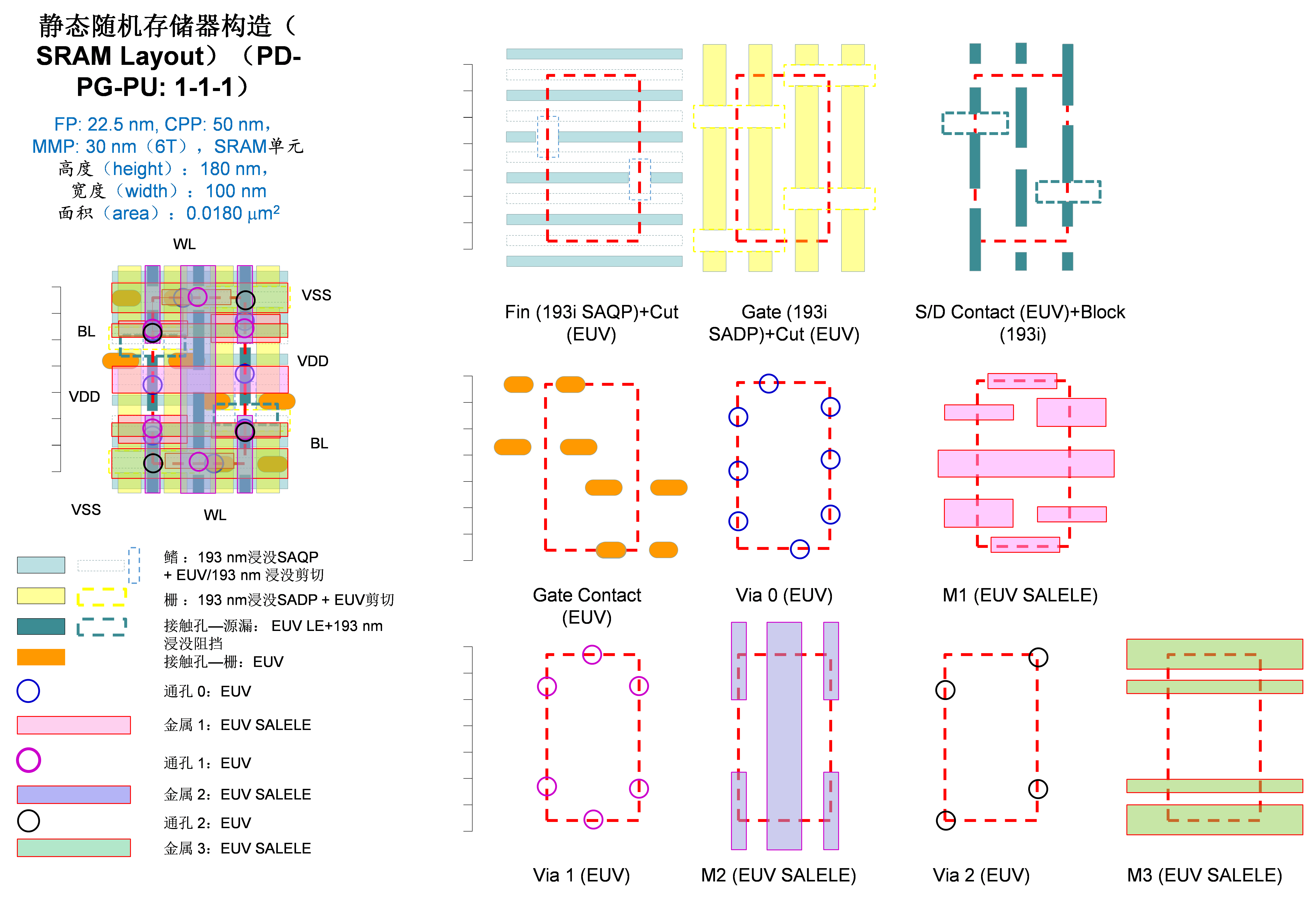
With the introduction of EUV lithography, the photolithographic process in 5 nm logic process can be simplified to use mostly single exposure method. In a typical 5 nm logic process, the contact-po...
Authors: Peng Zheng, Hai-Shi Wang
Institution:Chengdu University of Information Technology, Chengdu
Keywords:low dropout regulator (LDO);dual micro-power;ultra
doi:10.33079/jomm.19020402
Abstract:
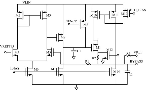
This paper presents a dual micro-power 150mA ultra LDO CMOS regulator, which is designed for high performance and small size portable wireless devices. The proposed LDO has been designed and simula...
Authors: Sicong Wang, Jian Mi, Abhishek Vikram et al.
Institution:Yangtze Memory Technologies Co, ., Ltd, Wuhan
Keywords:VIA;Dishing;AFM;Image;Metrology;3D NAND
doi:10.33079/jomm.19020403
Abstract:
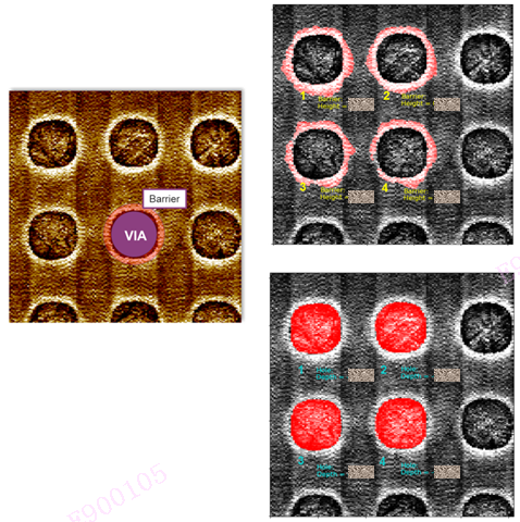
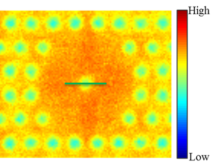
3D NAND (three-dimensional NAND type) has rapidly become the standard technology for enterprise flash memories, and is also gaining widespread use in other applications. Continued manufacturing pro...
Authors: Baolin Zhang, Yu Chen, Shisheng Xiong
Institution:School of Information Science and Technology, Fudan University, Shanghai
Keywords:Micro-phase;blending;lamellar pattern;solvent annealing;sequential infiltration synthesis
doi:10.33079/jomm.19020404
Abstract:
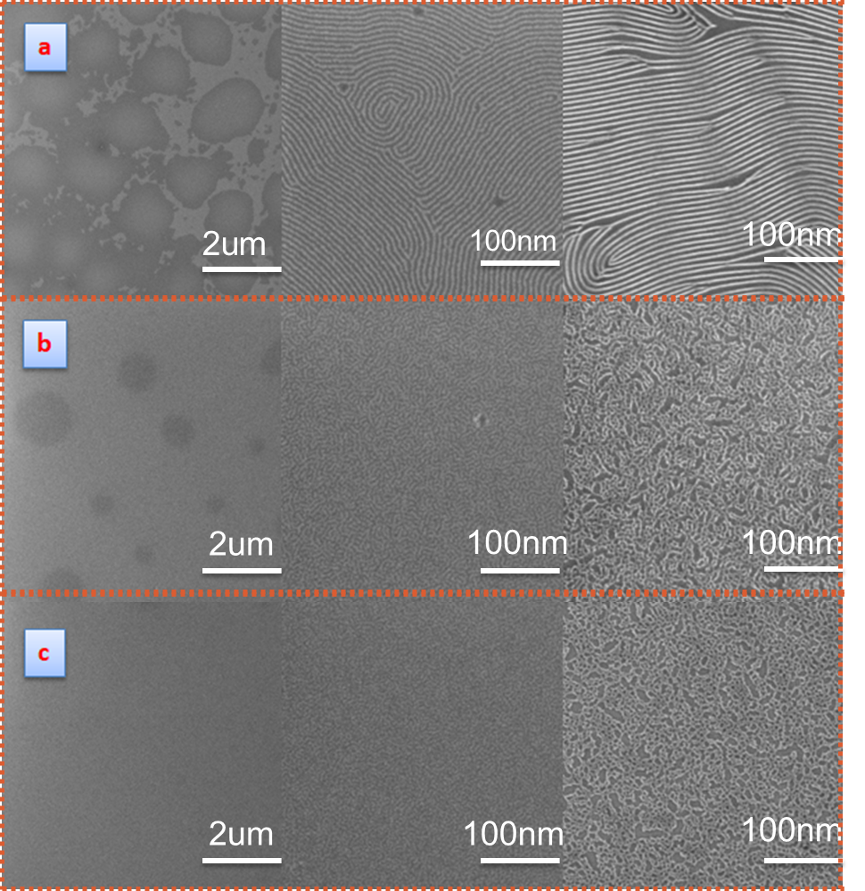
Directed Self-Assembly (DSA) of block copolymers (BCPs) is a promising technique for sub-10 nm nanofabrication, which is highly compatible with conventional lithography. DSA relies on the microphas...
Authors: Enming Shang, Yu Ding, Wenqiao Chen et al.
Institution:Shanghai IC R, &, D Center, Shanghai
Keywords:5 nm;FinFET;fin profile;semiconductor
doi:10.33079/jomm.19020405
Abstract:
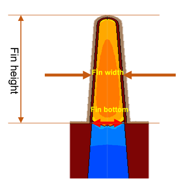
In 5 nm technology node, FinFET device performance is sensitive to the dimension of the device structure such as the fin profile. In this work, we simulate the influence of fin height and fin width...
Authors: Xiaoye Ding, Sicong Wang, Yi Zhou et al.
Institution:Yangtze Memory Technologies Co, ., Ltd, Wuhan
Keywords:WLI;Dishing;Metrology;3D NAND;Bonding
doi:10.33079/jomm.19020407
Abstract:
In traditional 3D NAND design, peripheral circuit accounts for 20-30% of the chip real-estate, which reduces the memory density of flash memory. As 3D NAND technology stacks to 128 layers or higher...
Authors: Litho World
Keywords:Packaging;Testing Industry
doi:10.33079/jomm.19020409
Abstract:
China's IC industry has been flourishing in recent years, huge market demand together with government investments are the major driving forces for this development. The status and development momen...
