The Application of Polyimide used in Semiconductor Industry:A Review
Authors: Jikang Liu, Jia Wei, Chenye Li et al.Institution:Hubei University of Education
Keywords:Polyimide;photosensitive polyimide;usage method;protecting layer;insulation layer
doi:JOMM2025.0005.en
Abstract:
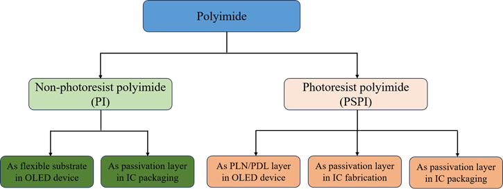
The polyimide (PI) and photosensitive polyimide (PSPI) were always regarded as protecting layer or insulation layer in semiconductor industry due to its high-temperature resistance, outstanding mec...
An Introduction on the IC Packaging Technology of FOPLP
Authors: Jikang Liu, Chenye Li, Jia WeiInstitution:Hubei University of Education
Keywords:FOPLP;die first;face up;face down;RDL first;die shift;panel warpage
doi:10.33079/jomm.25051001
Abstract:
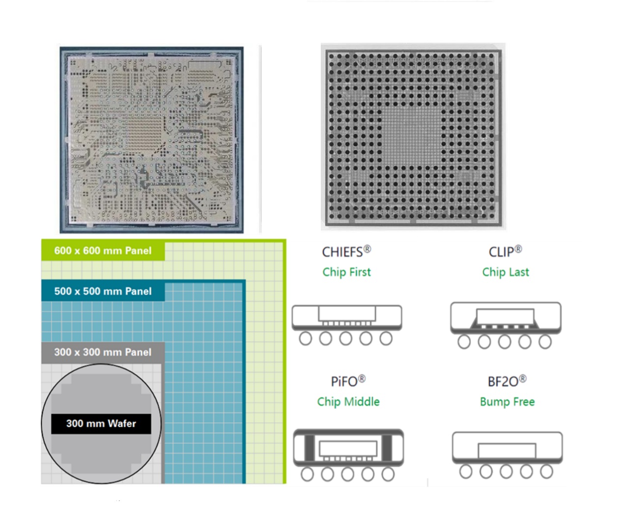
Based on the advantages of higher output efficiency, higher utilization, higher production, lower cost, no requirement for advanced process, higher device density, improved electrical performance a...
Influence of Parameters in the Design of a Faceted Structure for Incoherent Beam Shaping
Authors: Lihong Liu, Thierry Engel, Huwen Ding et al.Institution:Institute of Microelectronics, Chinese Academy of Sciences, Beijing
Keywords:Incoherent beam shaping;micro lens array;custom optimization
doi:10.33079/jomm.21040401
Abstract:
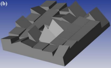
A reflective faceted structure is proposed to reshaping an incoherent light beam into two focalized spots. To obtain the desired irradiance distribution on a detector, custom optimization function ...
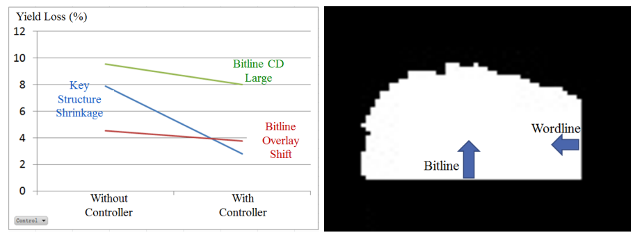
A Novel R2R Control Strategy with Virtual Structure Deployment and Rolling Wave Control Plan
Authors: Chang XuInstitution:Fujian Jinhua Integrated Circuit Co, ., Ltd, ., Jinjiang, Quanzhou, Fujian
Keywords:R2R;manufacturing;control;circuit design;virtual metrology
doi:10.33079/jomm.21040301
Abstract:
This paper presents an innovative R2R (run to run) control strategy. This novel approach has made use of circuit design structure through virtually put up the structure before reach the actual stru...
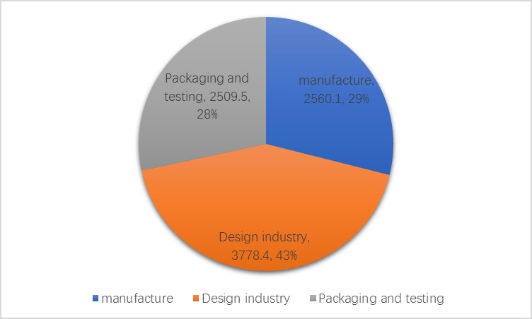
New Progress of China's Integrated Circuit Design Industry
Keywords:IC industry; Integrated Circuit Design Marketdoi:10.33079/jomm.21040203
Abstract:
China's IC industry has been flourishing in recent years, huge market demand together with government investments are the major driving forces for this development. The status and development momen...
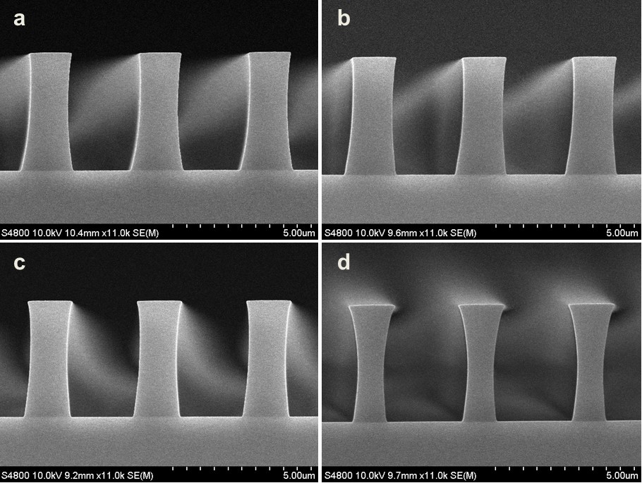
Improvement of Environment Stability of an i-Line Chemically Amplified Photoresist
Authors: Haibo Li, Qian Yang, Jia Sun et al.Keywords:Chemical amplification;thick film;i-Line;environment stability;Poly (p-hydroxyl styrene);PAB;PEB
doi:10.33079/jomm.21040201
Abstract:
An i-Line chemically amplified (ICA) thick film positive resist is reported in this paper. The impact of process conditions on photoresist performance was investigated. Pre-apply bake temperature a...

Patterning with Organized Molecules
Authors: Mark NeisserInstitution:Tan Kah Kee Innovation Laboratory
Keywords:Stochastics;Self-assembly;overlay;edge placement error;self-organizing;DNA origami;bottle brush polymers
doi:10.33079/jomm.21040202
Abstract:
Decades of progress in the semiconductor industry has led to lithographically printed dimensions that are small enough that the positions of individual molecules and the stochastic variation in the...
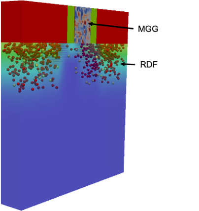
Nano-Electronic Simulation Software (NESS): A Novel Open-Source TCAD Simulation Environment
Authors: Cristina Medina-Bailon, Tapas Dutta, Fikru Adamu-Lema et al.Institution:Device Modelling Group, James Watt School of Engineering, University of Glasgow
Keywords:Integrated Simulation Environment;Variability;Drift-Diffusion;Quantum Correction;Kubo-Greenwood;Non-Equilibrium Green’s Function
doi:10.33079/jomm.20030404
Abstract:
This paper presents the latest status of the open source advanced TCAD simulator called Nano-Electronic Simulation Software (NESS) which is currently under development at the Device Modeling Group ...
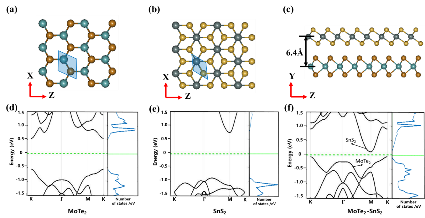
First-principles Simulations of Tunneling FETs Based on van der Waals MoTe2/SnS2 Heterojunctions with Gate-to-drain Overlap Design
Authors: Kun Luo, Kui Gong, Jiangchai Chen et al.Institution:Key Laboratory of Microelectronics Device and Integrated Technology, Institute of Microelectronics of Chinese Academy of Sciences
Keywords:2D materials heterojunction;tunnel-FET;gate-to-drain overlap;DFT-NEGF
doi:10.33079/jomm.20030405
Abstract:
The electronic properties and transport properties of MoTe2/SnS2 heterostructure Tunneling FETs are investigated by the density functional theory coupled with non-equilibrium ...
Material Modeling in Semiconductor Process Applications
Authors: Boris A. Voinov, Patrick H. Keys, Stephen M. Cea et al.Institution:Logic Technology Development, Intel Corporation, Hillsboro OR
Keywords:TCAD;atomistic modeling;density functional theory;molecular dynamics;kinetic Monte Carlo
doi:10.33079/jomm.20030406
Abstract:
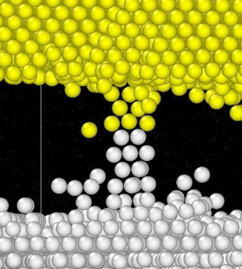
During the past decade, significant progress has been achieved in the application of material modeling to aid technology development in semiconductor manufacturing companies such as Intel. In this ...
