
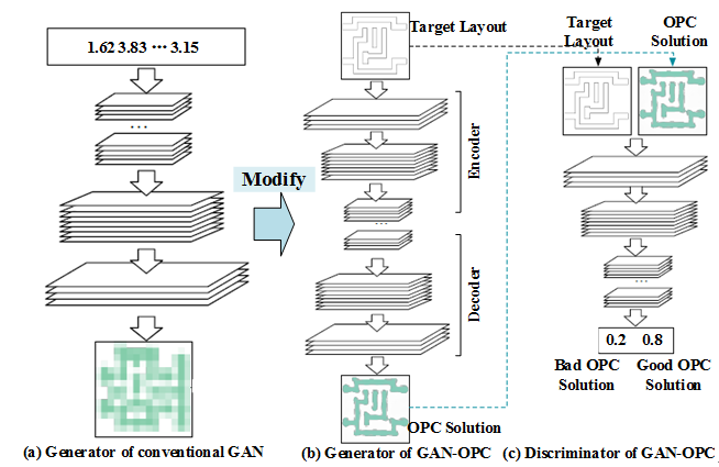
Study of Inverse Lithography Approaches based on Deep Learning
Authors: Xianqiang Zheng, Xu Ma, Shengen Zhang et al.Institution:Key Laboratory of Photoelectronic Imaging Technology and System of Ministry of Education of China, School of Optics and Photonics, Beijing Institute of Technology, China
Keywords:Computational lithography;inverse lithography technology (ILT);optical proximity correction (OPC);deep learning
doi:10.33079/jomm.20030301
Abstract:
Computational lithography (CL) has become an indispensable technology to improve imaging resolution and fidelity of deep sub-wavelength lithography. The state-of-the-art CL approaches are capable o...
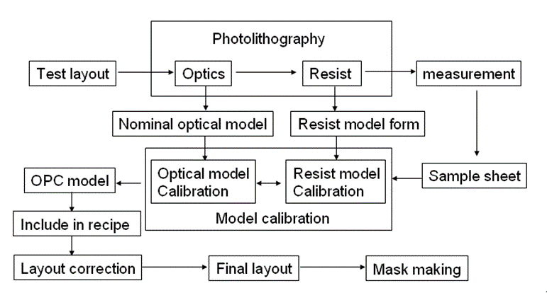
An Innovative Method to Improve Model Accuracy by Implementing Multi-models Scheme for 28nm Node and Below
Authors: Qingchen Cao, Tianhui Li, Shuying Wang et al.Institution:SiEn (QingDao) Integrated Circuits Co., Ltd
Keywords:Image quality;lithography;OPC model;multi-model
doi:10.33079/jomm.19020304
Abstract:
As the process comes into 28nm node and below, lithography struggles stronger between high resolution (high NA) and enough process window especially for hole layers (Contacts and Vias). Taking more...
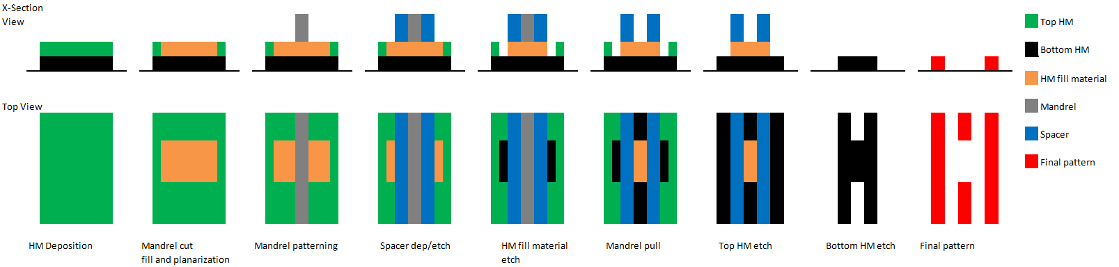
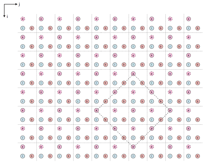
Innovation on Line Cut Methods of Self-aligned Multiple Patterning
Authors: Jeff ShuInstitution:GLOBALFOUNDRIES
Keywords:self-aligned multiple patterning;SAMP;self-aligned double patterning;SADP;self-aligned quadruple patterning;SAQP;line cut;edge placement error
doi:10.33079/jomm.19020301
Abstract:
Self-aligned multiple patterning (SAMP) can enable the semiconductor scaling before EUV lithography becomes mature for industry use. Theoretically any small size of pitch can be achieved by repeati...
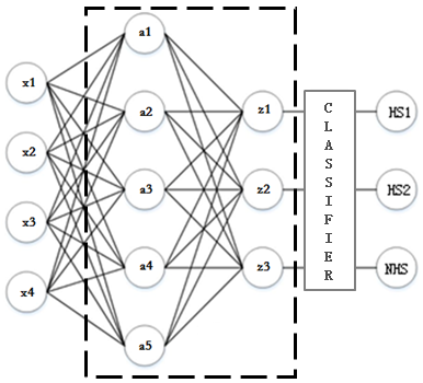
Hotspot Detection of Semiconductor Lithography Circuits Based on Convolutional Neural Network
Authors: Xingyu Zhou, Youling YuInstitution:Tongji University, Shanghai
Keywords:lithography;hotspot detection;CNN;deep learning
doi:10.33079/jomm.18010205
Abstract:
In the advanced semiconductor lithography manufacturing process, the sub-wavelength lithography gap may cause lithographic error and the difference between the wafer pattern and mask pattern which ...
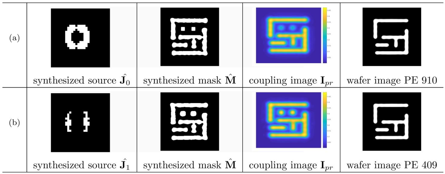
Variational Level-set Formulation for Lithographic Source and Mask Optimization
Authors: Yijiang Shen, Zhenrong ZhangInstitution:Guangdong University of Technology
Keywords:computational lithography;variational level set;source and mask optimization;coupling image
doi:10.33079/jomm.18010203
Abstract:
This paper addresses the contributing factors in lithographic source and mask optimization, namely, the accuracy of the image formation model and the efficiency of the inverse imaging calculations ...
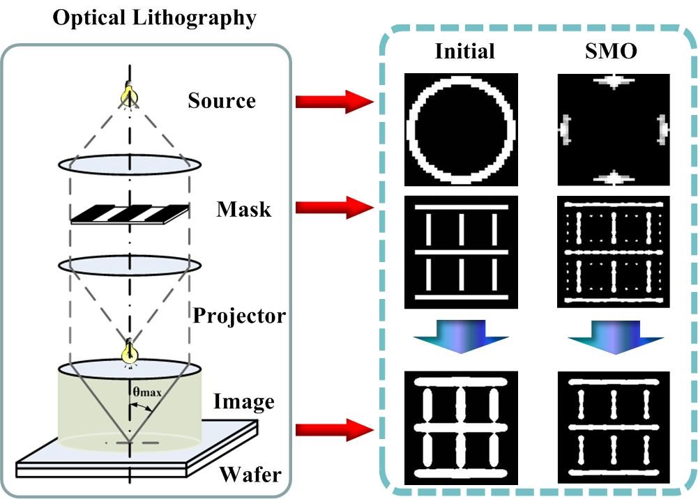
Compressive Sensing Approaches for Lithographic Source and Mask Joint Optimization
Authors: Xu Ma, Zhiqiang Wang, Gonzalo R. ArceInstitution:Key Laboratory of Photoelectronic Imaging Technology and System of Ministry of Education of China, School of Optics and Photonics, Beijing Institute of Technology, China
Keywords:Computational lithography;source mask optimization (SMO);compressive sensing (CS);inverse problem
doi:10.33079/jomm.18010202
Abstract:
Source and mask joint optimization (SMO) is a widely used computational lithography method for state-of-the-art optical lithography process to improve the yield of semiconductor wafers. Nowadays, c...
Hamamatsu’s Products for Optical Inspection, Metrology and Monitoring to Improve Yield and Accuracy for Semiconductor Processes
Authors: Chenghao Xiang, Xusheng ZhouInstitution:Hamamatsu Photonics (China) Co., Ltd., Beijing
Keywords:optical semiconductor inspection/metrology/monitoring solutions;image sensor;light sources;mini-spectrometer;photomultiplier tubes/modules
doi:10.33079/jomm.19020102
Abstract:
Pursuing small critical dimensions (i.e. 14 nm or below) and high integration bring us lots of physical defects causing low yield and functionality failures for foundries. Under this circumstance, ...
Development and Prospect of Process Models and Simulation Methods for Atomic Layer Deposition
Authors: Lei Qu, Rui Chen, Xiaoting Li et al.Institution:North China University of Technology, China
Keywords:thin film deposition;atomic layer deposition;growth model;prediction model;simulation method
doi:10.33079/jomm.19020204
Abstract:
Thin film deposition is one of the most important processes in IC manufacturing. In this paper, several typical models and numerical simulation methods for thin film deposition and atomic layer dep...
Analysis of Current Research Status of Plasma Etch Process Model
Authors: Xiaoting Li, Rui Chen, Lei Qu et al.Institution:North China University of Technology
Keywords:plasma etching;etching model;simulation
doi:10.33079/jomm.18010104
Abstract:
This paper summarizes the status of the plasma etch process modeling research. It mainly introduces typical etching models employing the analytical method, geometric method, system identification m...
The Variables and Invariants in the Evolution of Logic Optical Lithography Process
Authors: Qiang WuInstitution:Shanghai IC R, &, D Center, Shanghai
Keywords:image projection photolithography;imaging contrast;exposure latitude;mask error factor;linewidth uniformity;chemically amplified photoresist;phase shifting mask;optical proximity correction;and photoacid diffusion length
doi:10.33079/jomm.19020101
Abstract:
Photolithography has been a major enabler for the continuous shrink of the semiconductor manufacturing design rules. Throughout the years of the development of the photolithography, many new techno...